


Advanced Packaging Takes Center Stage
Knowledge is power, so the saying goes. In our modern context, this aphorism is alive and well in the form of the AI data center, where a host of technology companies vie for the power that comes with being the dominant knowledge broker in the ever-evolving information economy.
Underpinning these ambitions is an insatiable demand for computing power, only possible due to Moore’s Law and the ever-shrinking transistor scales modern chips have been able to achieve. As transistor density reaches its physical limits, however, advanced packaging has taken center stage in the race to make computer chips – and by extension the AI models they power – better and better.
In simple terms, advanced packaging involves bringing together multiple chips in a single integrated bundle, or package. Nevertheless, engineering this solution is anything but simple as it involves innovative engineering techniques, advanced equipment, and novel infrastructure. In particular, advanced packaging processes necessitate manufacturing techniques that are typically performed at front-end fabs rather than traditional packaging, assembly, and test facilities that have typically dominated the back-end stage in the chip manufacturing value chain.
As semiconductor manufacturers scramble to meet this moment – driven by lucrative AI demand – requirements for advanced packaging capabilities are reshuffling infrastructure needs, offering companies a unique opportunity to alter their facility footprints and potentially even their business models. Combined with recent geopolitical shifts and generous government subsidies, the moment has never been more acute for back-end manufacturing to evolve across a variety of facility approaches.
Rewriting The Packaging Playbook
Though the semiconductor value chain is often neatly bifurcated into front-end and back-end manufacturing, advanced packaging is breaking that neat distinction. Leading-edge foundries TSMC and Intel have together allocated tens of billions of dollars of investments into advanced packaging R&D, building pilot lines and low-volume capacity to serve burgeoning demand.
In July 2024, TSMC put a finer point on the topic by announcing their Foundry 2.0 strategy, with the intention to integrate advanced packaging processes into the scope of their traditional front-end foundry services, increasing their total addressable market and earmarking a greater percentage of their capex to packaging R&D. As industry analyst and Semiconductor Business Intelligence author Claus Aasholm noted, “From a strategic perspective, advanced packaging is becoming incredibly important and the main driver behind the Foundry 2.0 Strategy”.
TSMC’s proprietary advanced packaging solution Chip-on-Wafer-on-Substrate (CoWoS) / source: CNN, June 7, 2025
TSMC aims to provide capacity for 75,000 CoWoS per month by the end of 2025, a marked increase in capacity over previous years, but still not enough to meet demand. As volumes continue to scale, however, TSMC has made it clear that it has no interest in continuing to scale up production itself, but has instead sought partnerships with traditional back-end players. Amkor’s decision to invest $2 billion in a state-of-the-art facility in Peoria, AZ, was largely predicated on the complementary investment of TSMC, who is their lead customer, and an MOU the two companies signed to have Amkor package TSMC’s chips.
Co-location is made possible in part due to changing labor dynamics, as highly automated back-end processes put less emphasis on the labor economics typically associated with back-end facilities (accounting for the geographic footprint of traditional back-end sites which skews heavily towards Southeast Asia). Additionally, companies can benefit from the economic effects of proximity – workforce training programs, infrastructure and power investments, and supply chain resilience.
The co-located partnership model currently playing out in Arizona is a great example of how advanced packaging is creating new models for semiconductor facility investment, but it is only the most prominent. Across the semiconductor industry, accelerating demand for advanced packaging solutions will require more than just the heavyweight foundries to play a role, extending opportunities to legacy back-end players and other front-end fab manufacturers looking to optimize cleanroom utilization.
Advanced Packaging Capacity Solutions
According to Bain Capital’s 2024 Technology Report, “If data center demand for current-generation GPUs doubled by 2026, suppliers of key components would need to increase their output by 30% or more in some cases. This pull-through in demand will be concentrated in advanced packaging and memory, with makers of chip-on-wafer-on-substrate (CoWoS) packaging components needing to almost triple production capacity by 2026.”
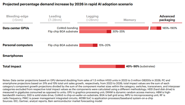
Surging demand for AI computing power will strain the supply chains for data center chips, personal computers, and smartphones / source: Bain Capital, 2024
With so much demand and still limited supply, where does the answer lie? One solution is for the standard business models of foundries and IDMs to evolve along with technology advancements. A report published by Boston Consulting Group in May 2024 noted that mature-node foundries, legacy OSATs, and IDMs are all threatened by advanced packaging’s new paradigm, but that each can still have a role to play in this emerging ecosystem.
In each case, more facility space for advanced packaging processes will need to be found. Advanced packaging facilities require infrastructure more akin to front-end fabs, with TSMC’s CoWoS facilities needing specialized equipment for silicon interposer manufacturing, including high-precision lithography tools for creating ultra-fine interconnects. This speaks to another aspect of advanced packaging facilities – equipment costs and installation are by far the biggest consideration, making both greenfield and brownfield options viable depending on other strategic imperatives.
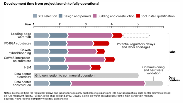
Lead times for fabs are years long, and advanced packaging is no exception / source: Bain Capital, 2024
Greenfield facilities, such as the aforementioned Amkor Arizona site and SK Hynix’s $4 billion announcement for a site in Indiana, allow manufacturers peak flexibility in regard to location, helping companies maximize synergies from co-location with other companies, workforces, and/or research institutions.
Brownfield sites, by contrast, naturally limit geographic flexibility to where they already exist, but offer a substantial time-to-market advantage that is all the more pressing in the context of accelerating AI demand. GlobalFoundries’ investments into its existing New York fab and Intel’s investments into its New Mexico campus are both examples of companies that saw the value in retrofitting existing infrastructure rather than trying to build from scratch.
Looking forward to additional capacity, we believe brownfield retrofits will have to provide a significant solution to meet existing unmet demand. Substantial underutilization of mature-node fabs across the world offers an opportunity for savvy IDMs and foundries to begin forging partnerships with advanced packaging providers, allocating a portion of facility space that can be neatly retrofit in exchange for supply agreements with advanced packaging suppliers.
The enhanced value of being in proximity to leading-edge foundries puts a greater premium on brownfield sites in Arizona near TSMC’s expansion and near Intel’s leading-edge sites as they develop their Foveros packaging competitor. Combined with geopolitical tailwinds to regionalize more semiconductor manufacturing, advanced packaging is likely to start a trend that sees a higher proportion of back-end facilities expanding to the United States, China, and Taiwan.
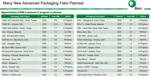
Source: BESI Investor Day presentation, June 12, 2025
Looking Ahead – What’s Next For The Back-End?
Advanced packaging has long been foreseen as the next step in the evolution of Moore’s Law, but even those intimately familiar with the AI industry have been surprised at how quickly demand has grown. NVIDIA’s ascendance to the most valuable technology company in the world is the tailwind driving both the AI and semiconductor industry growth in parallel, and creating opportunities for advanced packaging.
Though this new era of packaging technology is dominated by the mega-firms with the capital to support it, notably TSMC, the packaging volumes needed to support AI computing workflows mean that the facility requirements are already beyond what TSMC and its partners can provide. Now is a moment for well-resourced legacy OSATs such as ASE to expand their facility presence, for underutilized mature-node foundries to service demand with front-end cleanrooms, and for even IDMs to adjust their business model by integrating more advanced packaging processes in their fabs today, in partnership with technology leaders.