


NEWPORT, UK FAB SALE NOW COMPLETE
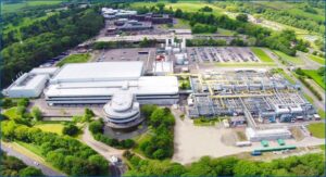 ATREG is pleased to announce that the acquisition of Nexperia B.V.’s operational 200mm wafer fab located in Newport, South Wales, UK by Vishay Intertechnology, Inc. has officially closed. Located on the UK’s largest semiconductor site and one of the top five semiconductor clusters in Europe, this facility is the largest manufacturing fab in the UK. Vishay will keep the asset operational and preserve local jobs.
“This acquisition enables Nexperia to transition the Newport wafer fab in South Wales to a new owner who can ensure the long-term future of the site,” explains Stephen Rothrock, founder and CEO of ATREG. “The facility will continue to play a crucial role in the local Welsh semiconductor ecosystem. Congratulations to both companies on a successful outcome!”
Click here to read our full press release. Click here to read Vishay’s press release.
CHIPS ACT FUNDING – WILL THE BACK-END BE LEFT OUT?
By E. Jan Vardaman, Founder & President, TechSearch International, Inc.

For the past couple of years, governments around the world have been heavily investing to bring semiconductor manufacturing back to their shores. In the United States, the CHIPS & Science Act provides $52 billion in subsidies for domestic semiconductor R&D, granted via the Department of Commerce (DOC). In addition, there are financial incentives available from the Departments of Defense (DOD) and Energy (DOE). An investment tax credit of 25% is offered for investments in semiconductor manufacturing and processing equipment. While advanced fabs have received the most attention under the CHIPS Act, legacy fabs and packaging will also be funded under the program. But with such a lion’s share of public funding mostly focusing on the front-end and only a small portion of the total spending has been targeted at packaging, assembly, and test so far and it raises concerns – does the back-end run the risk of being underfunded?
The DOC’s $39 million incentive program offers direct funds as grants or loans to invest in U.S. production of strategically important semiconductor chips to ensure a sufficient sustainable and secure supply of older- and current-generation chips for national security purposes and critical manufacturing industries. There is an allocation of $11 billion to strengthen U.S. semiconductor R&D leadership to catalyze and capture the next set of critical technologies, applications, and industries.
So far, the U.S. Chips Program Office (CPO) under the DOC has signed a pact to provide $35 million to military contractor BAE Systems to expand an existing chip facility in New Hampshire that makes parts for F-35 fighter jets. The CPO also agreed to provide $162 million to Microchip Technology to help boost its U.S. production of microcontrollers that are also used in defense equipment. Funding of $2 billion for the DOD Microelectronics Commons is targeted to establish a national network that will create direct pathways to commercialization for U.S. microelectronics researchers and designers from “lab to fab.” Workforce development initiatives underpin all programs.
On February 19th, GlobalFoundries announced it will be receiving $1.5 billion from the U.S. CHIPS and Science Act, with additional awards to foundries anticipated over the next few weeks. On March 14th, it was reported that Samsung was poised to receive over $6 billion in CHIPS Act grants to fund its expansion beyond its project in Texas.Several companies have received DOD funding for substrates, including Calumet Electronics Corporation ($39.9 million) and GreenSource Fabrication LLC ($46.2 million). Osceola County where Skywater Technology is located may receive up to $289 million for advanced packaging.

On the back-end side, the National Advanced Packaging Manufacturing Program (NAPMP) has been allocated $2.5 billion, with a focus on strengthening semiconductor advanced test, assembly, and packaging capability in the domestic U.S. ecosystem. The NAPMP will make R&D investments that leverage existing areas of strength including design and simulation tools, manufacturing equipment (used to implement many wafer-based fab processes necessary for advanced packaging), and R&D capabilities in relevant areas to advanced packaging, including novel materials, wide-bandgap and ultra-wide-bandgap semiconductors, novel memory, and photonics (used along with heterogeneous integration to build advanced, highly functional systems). As outlined in the NAPMP Vision Paper [1], its goals are to:
- Enable successful advanced packaging development efforts to be validated and transitioned at scale to U.S. manufacturing
- Develop packaging platforms capable of both high-volume and customized manufacturing
- Create an advanced packaging ecosystem based on heterogeneous chiplet technology to promote widespread and easy use of the technologies developed
- Bolster advanced packaging workforce development efforts to sustain the domestic ecosystem
NAPMP will include an Advanced Packaging Piloting Facility (APPF) where successful development efforts will be transitioned and validated for scaled transition to U.S. manufacturing in high volume. Investments will be made in six priority areas – materials and substrates; equipment, tools, and processes; power delivery and thermal management; photonics and connectors; chiplet ecosystem development; and co-design with automated tools.
As outlined in IPC’s Analysis of the North American Semiconductor and Advanced Packaging Ecosystem report published in July 2021, simply fabricating semiconductors in the United States and sending them to Asia for packaging and assembly does not shorten the supply chain, it actually lengthens it. A complete ecosystem is required. Hopefully, additional funding for the full ecosystem will be announced in the near term.
We will keep track of additional CHIPS & Science Act funding announcements as they are made public over the next several months. In the meantime, click here for the latest Q1 2024 edition of TechSearch International’s quarterly Advanced Packaging Update.
[1] S. Iyer, “The Vision for the National Advanced Packaging Manufacturing Program,” www.nist.gov, November 20, 2023.
About E. Jan Vardaman
 Jan is Founder and President of TechSearch International, Inc., a U.S. technology licensing and consulting firm based in Austin, TX specializing in the electronics industry. She is the co-author of How to Make IC Packages with Nikkan Kogyo Shinbunsha, a columnist with Printed Circuit Design and Fab/Circuits Assembly and the author of numerous publications on emerging trends in semiconductor packaging and assembly. Jan served on the NSF-sponsored World Technology Evaluation Center (WTEC) study team involved in investigating electronics manufacturing in Asia as well as on the U.S. mission to study manufacturing in China. She is a senior member of IEEE EPS and an IEEE EPS Distinguished Lecturer. Jan is a member of SEMI and SMTA as well as an IMAPS Fellow. She received the IMAPS GBC Partnership award in 2012, the Daniel C. Hughes, Jr. Memorial Award in 2018, and the Sidney J. Stein International Award in 2019. Before founding TechSearch International in 1987, she served on the corporate staff of Microelectronics and Computer Technology Corporation (MCC), the electronics industry’s first pre-competitive research consortium.
ATREG TO SPEAK AT GSA’S TECH SUMMIT
ATREG has been invited to present at the GSA TECH Summit to take place on April 30th at Samsung’s headquarters in San Jose, CA. ATREG Senior Vice President Annie Rothrock will share insightful perspectives on the current global semiconductor manufacturing landscape, touching on such topics as:
 Fab investment trends – Where has the industry been and where is it headed?
- Geopolitical uncertainty – How are companies responding to increased government scrutiny? How are governments working to entice greater investment?
- Technological shifts – How are innovations such as compound semiconductors, artificial intelligence, and electric vehicles impacting how companies are planning for future production?
- Capacity constraints – How are companies responding to underutilization among their fabs?
- Capex considerations – What factors are influencing companies to choose between foundries, greenfield investments, or brownfield refurbishments?
Click here to register for the event.
By Malcolm Penn, Chairman & CEO, Future Horizons
Artificial intelligence (AI) is up front and center of every firm’s dream, in a torrent of hope, hype, and hysteria not seen since the late 1990s Internet-driven Dot-com boom. No company, however, has benefited more than nVIDIA, which has seen its share price increase by almost 400% since the start of 2023. As a result, nVIDIA’s market capitalization, at US$1.8 trillion, has leapfrogged Alphabet to become the third most valuable U.S. company after Microsoft and Apple, despite the fact that Alphabet’s net income was greater than nVIDIA’s total revenues.

Right now, only a few brave souls dare to bet against nVIDIA’s market value rising further, as stock market investors swoon at dreams of its AI-overlord future. With year-to-date stock gains of close to 50%, dwarfing the 5% S&P 500 index rise, the industry has run out of superlatives to describe the AI chip juggernaut. At the risk of raining on the AI parade, we are fearful that the current AI hype has all of the echoes of the 2000 Dot-com euphoria and, just as then, no one believes a bust is coming. But, when a tech CEO asks for trillions, not billions, when raising funds for an AI chip project, you know, deep down in your heart of hearts, that this sector is getting a little bit too hot.
In addition, nVIDIA’s current valuation defies market rationale, implying the company will be able to maintain its monopolist-like sales and profit margin for the next decade, whilst simultaneously growing sales tenfold, from its current US$60 billion level to more than US$600 billion. To put that into context, the entire chip industry sold US$527 billion in 2023, a figure that is forecast to grow to US$1.4 trillion in this timeframe.
For the good times to keep rolling, the law of large numbers must cease to apply, and competition, innovation, and pricing pressure will not come to bear until at least the mid-2030s. Never forget too that AI is an enabler and not a product per se and, whilst it will undoubtedly transform many industries and the way people work, the road to this end goal is currently unclear and will certainly take a lot longer than the current exuberance implies.
About Malcolm Penn
 Malcolm is the Founder of Future Horizons, a leading global semiconductor industry analyst firm based in Sevenoaks, UK. He has over 55 years of experience in the semiconductor and electronics industry, from advanced research and manufacturing to applications, during which he has held various operations, marketing, and business development positions. Malcolm serves as a member of ATREG’s Advisory Board. He holds a BSc Honors degree in Electronic Engineering from the University of London, UK.
CONNECT WITH ATREG AT UPCOMING INDUSTRY CONFERENCES
 Members of the ATREG team look forward to reconnecting with you at upcoming global industry conferences over the coming few months. Whether your company seeks to acquire or sell a brownfield wafer fab or select the best location for a brand-new greenfield facility, please don’t hesitate to email us to set up an appointment with one of our fab transaction advisors and discuss your semiconductor infrastructure-rich manufacturing asset needs. We hope to see you there!
- GSA TECH Summit, April 30, San Jose, USA
- Display Week, May 20-22, San Jose, USA
- JP Morgan Global Tech, Media & Communications Conference, May 20-22, Boston, USA
- ITF World, May 21-22, Antwerp, Belgium
- Stifel Cross-Sector Insight Conference, June 4-6, Boston, USA
- Bank of America Merrill Lynch Global Technology Conference, June 4-6, San Francisco, USA
- GSA European Executive Forum, June 18-19, Munich, Germany
- SEMICON West, July 9-11, San Francisco, USA