


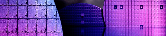
ATREG FACILITATES SALE OF ONSEMI’S PA FAB TO SILEX ATREG is pleased to announce that it has successfully assisted onsemi with the sale of its 200m operational fab located in
More »
ATREG FACILITATES SALE OF ONSEMI’S PA FAB TO SILEX ATREG is pleased to announce that it has successfully assisted onsemi with the sale of its 200m operational fab located in
More »

GLOBAL FAB ASSET MARKET HEATING UP The global semiconductor market is entering a new phase, with global semiconductor sales continuing to climb toward the projected $1 trillion mark. According to
More »
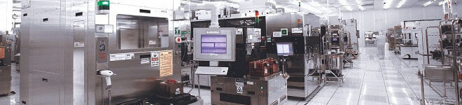
GLOBAL SEMI FABS AVAILABLE FOR SALE As the new year gets underway, momentum is building across the global semiconductor manufacturing asset market. Increased activity and renewed investment interest are creating
More »

EXECUTIVE Q&A: JOHN NEUFFER, PRESIDENT & CEO, SIA ATREG recently sat down with John Neuffer, President and CEO of the Semiconductor Industry Association (SIA) headquartered in Washington D.C., to discuss
More »
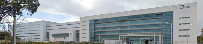
JDI HIGASHIURA FAB SALE TO SONY NOW COMPLETE ATREG is pleased to announce that the acquisition of Japan Display, Inc. (JDI)’s large operational LCD panel manufacturing fab located in Higashiura,
More »