


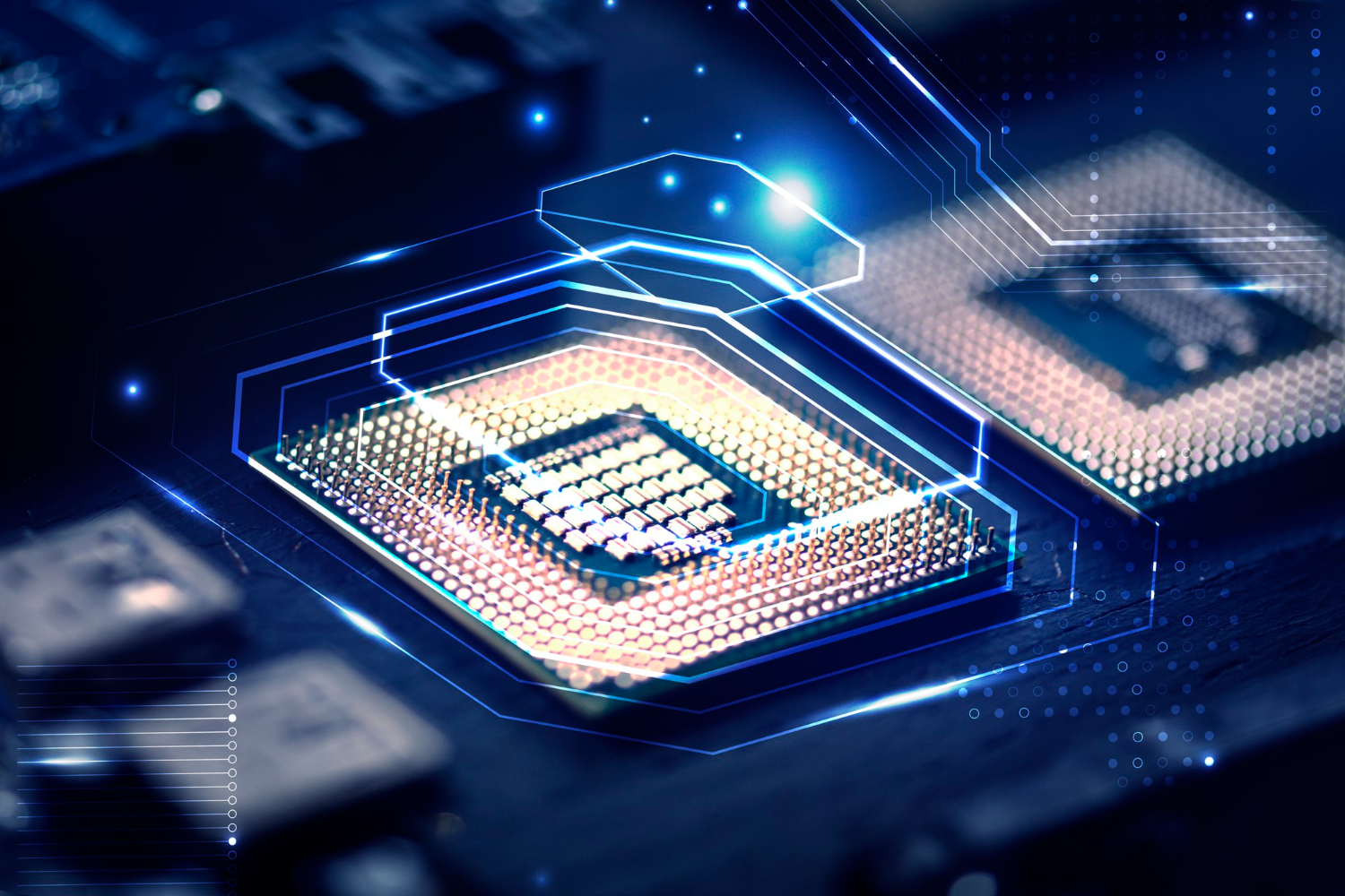
GLOBAL FAB ASSET MARKET HEATING UP
The global semiconductor market is entering a new phase, with global semiconductor sales continuing to climb toward the projected $1 trillion mark. According to the latest industry figures just released by the Semiconductor Industry Association (SIA), global chip sales amounted to $88.8 billion last February, 7.6% more than January 2026 and 61.8% more than February 2025, boosted by APAC, the Americas, and China.
 Increased activity and renewed investment interest are creating timely opportunities for companies looking to expand or reposition their chip manufacturing capabilities. ATREG is seeing strong global demand play out in real time as we are experiencing increasing requests for fab dispositions to acquisitions to capacity sharing partnerships and site selection. Should your company seek to acquire a manufacturing facility in the coming months, please feel free to email ATREG Vice President Stuart Smith to set up a conference call to discuss your specific global infrastructure-rich manufacturing asset needs and review our current diverse portfolio of available offering opportunities, including 200mm and 300mm cleanrooms with loading and supply agreements available in the U.S. and Europe.
EXECUTIVE Q&A WITH JODI SHELTON, GSA
![]() ATREG recently sat down with Jodi Shelton, Co-founder and CEO of the Global Semiconductor Alliance (GSA) to discuss GSA’s key role within the global semiconductor ecosystem as well as the key challenges our industry is facing.
ATREG recently sat down with Jodi Shelton, Co-founder and CEO of the Global Semiconductor Alliance (GSA) to discuss GSA’s key role within the global semiconductor ecosystem as well as the key challenges our industry is facing.
Take us back to 1994. You went from studying philosophy to working for a fabless semiconductor company to joining a dinner with fabless CEOs that became the Fabless Semiconductor Association (FSA). What did you see that others didn’t, and did you have any idea what you were setting in motion?
Before founding the organization, I was working at a fabless semiconductor company preparing for an IPO. During the roadshow, investors repeatedly asked not if, but when the company would build fabs. Yet the entire premise of the company and many others like it was to remain fabless. It became clear that there was a broader, underrecognized movement of companies committed to this model, despite skepticism from Wall Street and the industry. After leaving, I became convinced that if fabless CEOs came together, we could shift that perception. I pushed hard to convene them even showing up uninvited to secure a meeting with a key CEO and eventually that led to a dinner that became the foundation of the organization. Fifty companies joined at launch in 1994. At the time, most investors believed fabless was temporary. I ignored that conventional wisdom and moved forward anyway, despite being in my twenties and lacking any traditional path to lead such an effort. In hindsight, it worked because the model was already inevitable; it just needed a collective voice.
Over the past three decades, how has GSA’s mission shifted as the line between “fabless” and “fab” has blurred, particularly as hyperscalers and OEMs now design their own silicon and engage directly with foundries?
GSA has never stood still. We have consistently evolved in response to where the industry was going. We began by helping fabless companies collectively establish credibility. Once that was achieved, we expanded to include foundries, OSATs, and EDA companies because the ecosystem is inherently interdependent. In 2001, we transitioned from FSA to GSA to reflect a global reality and avoid becoming narrowly defined by one business model. That shift was about staying relevant before change became necessary. Later, we expanded again to include systems, software, solutions, and services companies such as Microsoft, Meta, Amazon, and Tesla because they were increasingly shaping semiconductor demand and design. The goal has always been simple: anyone meaningfully influencing the semiconductor ecosystem should have a seat at the table. Each expansion was debated, but each one strengthened the relevance of the organization.
 From GSA’s vantage point across the broader ecosystem, what do you see as the most pressing capacity or supply chain challenges facing the industry right now?
The industry’s key constraints are capacity, memory, energy, and talent. Capacity remains the most immediate issue, especially the imbalance between leading-edge and mature nodes and geographic concentration. AI-driven demand is intensifying this pressure. Memory is becoming a structural bottleneck as AI workloads increase bandwidth and performance requirements faster than supply can respond. Energy is now a critical gating factor for both fabs and data centers, influencing where expansion is even feasible. Underlying all of this is talent and infrastructure which are required to sustain long-term growth. The challenge has shifted from simply expanding capacity to managing a more complex set of interdependencies across the ecosystem to ensure long-term resilience and scalability.
Government incentive programs such as the U.S. CHIPS Act, the EU Chips Act, and similar initiatives in Japan, South Korea, and India have reshaped the calculus around where new fabs get built. Is there a gap between what policymakers think these programs will accomplish and what you’re actually hearing from members?
There is a clear gap between policy intent and industry execution. Programs such as the CHIPS Acts in the U.S., the EU, and elsewhere have successfully elevated semiconductors as a strategic priority. However, incentives alone do not determine investment decisions or timelines. Members consistently point to execution challenges, including funding timelines and administrative complexity, which affect predictability in large-scale investments. More fundamentally, long-term location decisions are driven by structural factors such as energy availability, talent, permitting speed, and ecosystem maturity, areas where Asia still holds advantages in many segments. Finally, companies are looking beyond initial incentives to long-term sustainability, including workforce development and ongoing ecosystem support. That continuity is still uncertain in many regions.
AI has been the dominant demand driver in semiconductors over the past two years, fueling massive investments in leading-edge capacity. But there’s a growing conversation about whether AI’s impact extends beyond advanced logic and HBM into more mature process nodes, things such as power management, sensors, and analog. Do you agree, and how do you see AI reshaping demand across the full spectrum of semiconductor manufacturing?
AI is clearly driving demand at the leading edge, especially in advanced logic and HBM, but its impact is much broader and still unfolding across the rest of the semiconductor ecosystem. While advanced compute is central, AI systems rely heavily on power management, analog, sensors, and connectivity, all of which are becoming more important as AI moves to edge such applications as automotive, industrial, and consumer devices. Power and energy efficiency are becoming design constraints. Sensors and analog are essential for bridging physical and digital environments. At the same time, AI is accelerating heterogeneous integration and advanced packaging, increasing demand across multiple nodes simultaneously. While the headlines tend to focus on the most advanced nodes, the reality is that AI is creating a more interconnected demand environment. It is reinforcing the importance of mature nodes and highlighting the need for a balanced and resilient supply chain that can support innovation at every level. In many ways, AI is not just a demand driver. It is a unifying force pulling the entire semiconductor ecosystem forward together.
GSA has long described itself as a neutral platform where companies from across the globe, including U.S. and Chinese firms, come together around shared industry interests. You’ve demonstrated that commitment in concrete ways, like convening conferences in Shanghai even during periods of heightened tension. How do you think about GSA’s role as a diplomatic bridge when the political environment is pulling in the other direction? And is that bridge more important now than ever or harder to maintain?
GSA has always believed that innovation in our industry depends on global collaboration, even when the geopolitical environment is challenging. Our role is not to take positions on policy, but to create a trusted environment where companies can come together around shared technical, business, and supply chain priorities. That neutrality is not passive; it is a form of thought leadership in its own right. There is real value in having a forum that helps define how the industry can continue to collaborate responsibly across borders, within the realities of different regulatory and national security frameworks. What we hear from our members across regions is a strong desire to stay connected. The semiconductor ecosystem is deeply interdependent. The need for connection and trust has not diminished. It has intensified. Yes, the bridge is harder to maintain in today’s environment, but it is also more critical. At the end of the day, this is a global industry. Companies want to participate in all markets and they need the ability to do so if they are going to continue to grow and succeed. Our responsibility is to foster that connection in a way that supports the long-term health and stability of the global semiconductor ecosystem.
Advanced packaging has emerged as one of the most strategically important areas in semiconductor manufacturing, arguably as critical as the node race itself. How do you see the advanced packaging ecosystem evolving, and what does it mean for collaboration between the design and manufacturing sides of the industry?
Advanced packaging has moved from a back-end function to a core driver of system performance. The industry is shifting toward system-level design, with chiplets and heterogeneous integration enabling more flexible architectures, but also greater interdependence across the ecosystem. As a result, foundries, OSATs, IDMs, and fabless companies must collaborate much earlier in the design process, with packaging now influencing architecture decisions from the start. Overall, advanced packaging is redefining innovation as an ecosystem effort.
 The global semiconductor industry has gone through dramatic cycles of consolidation over the past decade, yet there’s renewed energy around deep tech start-ups, particularly in AI hardware, photonics, and compound semiconductors. What’s the state of semiconductor entrepreneurship right now, and what does the start-up pipeline look like?
We are seeing a renewed wave of semiconductor start-ups, but with a different profile than in earlier cycles. Today’s start-ups are highly specialized, focused on areas such as AI hardware, photonics, compound semiconductors, and power efficiency often solving problems created by new system architectures. Barriers remain high due to capital intensity and long development cycles, but the ecosystem is more supportive than before, with more strategic investment and earlier collaboration with incumbents and foundries. Success now depends less on scale at inception and more on deep integration into the broader ecosystem early in development. Overall, the pipeline is smaller, but more strategically aligned with where the industry is heading.
You’ve been pulling back the curtain on some of the industry’s most influential leaders in your “A Bit Personal” podcast. What’s surprised you most about what you’ve heard?
What has been most striking is how much depth exists behind public success. Across leaders, there is a consistent pattern of resilience, curiosity, and non-linear career paths. Many did not follow traditional trajectories, but instead learned through risk-taking and experience. Equally important is the emphasis on relationships and trust. Even in a technology driven industry, success is often rooted in people, teams, and collaboration. There is also a surprising level of openness about challenges and failure, which is less visible in formal settings. Ultimately, what emerges is a shared sense of responsibility for the broader impact of the industry. That is really the goal of A Bit Personal: to humanize leadership and give people a more complete picture of what it takes to succeed, not just professionally, but personally as well.
Looking ahead three to five years, what is the one issue or trend you think the industry is underestimating, something you wish more leaders were talking about?
One of the most underestimated issues is the strain on the foundational systems required to support continued growth, especially capacity, memory, and energy, within an increasingly complex geopolitical environment. AI demand is driving massive investment in capacity, but the harder challenge is sustaining that growth across leading-edge and mature nodes, as well as across regions. Memory is emerging as a system-level bottleneck, not just a component challenge, as AI architectures evolve. Energy availability is becoming a critical constraint for both fabs and data infrastructure. At the same time, geopolitical friction is leading to supply chain regionalization, adding complexity to an already interdependent ecosystem. While the industry is rightly focused on innovation and growth, long-term success will depend on whether the underlying foundation and global operating environment can keep pace.
About Jodi Shelton
 Jodi Shelton is the co-founder and CEO of the Global Semiconductor Alliance (GSA). A pioneer within the technology space, Shelton was instrumental in the creation of the Alliance and has continuously addressed global issues in the industry as the voice of its members. Under her leadership, GSA has grown its membership to include companies throughout the supply chain representing 300+ corporate members on six continents and established the GSA Talent Initiative (GTI) and GSA Women’s Leadership Initiative (WLI). In her role as CEO, Shelton ensures that the Alliance remains focused on achieving its defined mission and goal to foster a more effective ecosystem through collaboration, integration, and innovation. She is the key liaison between GSA and the business community at high-level financial and industry conferences, providing insight on key topics pertaining to the global semiconductor supply chain. Shelton also serves on several boards, holds advisory positions, and hosts the podcast A Bit Personal, which features candid conversations with technology leaders, exploring the personal experiences that shape leadership and decision-making.
MEMORY’S MOMENT: WHY THE U.S. CAN’T AFFORT TO SIT OUT OF THE BIGGEST FAB BUILDOUT IN A GENERATION
The global memory chip industry is in the middle of the largest coordinated capacity buildout in its history. Samsung has committed a record $73 billion to chip capacity expansion and R&D in 2026 alone. SK Hynix placed a $7.9 billion order for cutting-edge EUV lithography equipment from ASML and is investing $13 billion in a new advanced packaging facility in Cheongju, South Korea. Micron’s capital expenditure will exceed $25 billion this fiscal year, with a planned step-up of more than $10 billion the following year. These are not incremental expansions. They are strategic bets on a structural transformation in semiconductor demand, one driven by AI infrastructure that shows no signs of slowing down.
 The numbers reflect a market in genuine disequilibrium. Both Samsung and SK Hynix warned in January that the memory supply crunch will persist through at least 2027, constrained by limited cleanroom space and explosive AI-driven demand. SK Group Chairman Chey Tae-won went further, estimating the shortage could last four to five years due to endemic constraints in semiconductor production. Memory pricing has responded accordingly – Samsung raised prices on certain DRAM modules by as much as 60% in a single quarter in late 2025, and the major memory producers have shifted from quarterly and annual pricing to multi-year supply contracts of three to five years with hyperscale customers. This is not a typical memory upcycle. The market’s own participants are signaling that the structural economics of memory have changed.
And yet, the overwhelming majority of this investment is flowing outside the United States. SK Hynix’s Yongin semiconductor cluster and Cheongju packaging complex are both in South Korea. Micron is building a $24 billion NAND fabrication facility in Singapore and a $9.6 billion HBM production plant in Hiroshima, Japan. Kioxia extended its Yokkaichi joint-venture with SanDisk through 2034, anchoring NAND production in central Japan. In China, CXMT is expanding its Shanghai plants to two to three times the capacity of its Hefei home base, while YMTC is dedicating half of a new Wuhan fab to DRAM and partnering on HBM assembly – aggressive moves enabled by a global supply crunch that has given emerging players room to grow. The U.S., despite being the world’s largest consumer of memory and the home market for many of its most important buyers, accounts for a strikingly small share of global memory production capacity.
The strategic risks of this concentration have never been more visible. South Korea – where Samsung and SK Hynix together control over 70% of the global DRAM market – imports 94% of its energy, routing roughly 70% of its crude oil through the Strait of Hormuz. The 2026 Iran conflict laid bare just how fragile that dependency is. The effective blockade of the Strait disrupted 20% of global oil supplies, sent the Korean won to a 17-year low, and triggered the KOSPI’s worst single-session decline in its 43-year history. The damage extended beyond energy prices: Qatar-sourced helium, a critical input for semiconductor manufacturing with no viable substitute, saw prices spike more than 40% after strikes on the Ras Laffan facility disrupted supply. South Korea’s government responded with a $17 billion supplementary budget to cushion the blow, but the episode underscored a structural vulnerability that no emergency spending package can fully resolve. As the Carnegie Endowment observed, the conflict is exposing the deep energy vulnerabilities of Korea’s chip industry – vulnerabilities that compound the geopolitical risks already inherent in concentrating so much critical manufacturing capacity in Northeast Asia.
There are early signs that the industry recognizes the need to diversify. SK Hynix filed for a U.S. Nasdaq listing in March 2026 and established a U.S.-based entity focused on AI investment and collaboration with American partners. Micron has accelerated timelines at its Boise, ID facilities and broken ground on a New York fab targeting production by 2030. But these are still modest steps relative to the scale of investment flowing to Korea, Japan, Singapore, and China.
 The opportunity for the United States is significant and time-sensitive. The CHIPS Act policy framework remains in place, infrastructure corridors and greenfield sites with the power, water, and workforce access required for memory class cleanroom are available, and – critically – demand from memory manufacturers for U.S.-based capacity options is rising. ATREG is observing a notable uptick in interest from both domestic and international memory manufacturers actively evaluating U.S.-based greenfield and brownfield capacity options – spanning DRAM, NAND, and emerging memory architectures. Site selection activity for memory class cleanroom is accelerating in ways we have not seen in over a decade.
The window, however, will not stay open indefinitely. The best-positioned sites, power allocations, and infrastructure corridors will be committed in the near term as the broader semiconductor industry competes for the same resources. Memory manufacturers assessing long-term capacity needs should be evaluating U.S. options now, while the policy environment is supportive and the strategic rationale has never been clearer. The supercycle is here. The question is whether the U.S. will be a meaningful part of it.
ADVANCED PACKAGING AT A FACILITY CROSSROAD
By Stephen M. Rothrock, Founder & CEO, ATREG, Inc.
 In this contributed viewpoint published in Semiconductor Packaging News‘ January 2026 issue, ATREG Founder & CEO Stephen Rothrock takes a look at how advanced packaging is impacting manufacturing fab decisions for chip makers.
The rise of advanced packaging from back-end afterthought to strategic imperative is forcing difficult facility decisions across the global semiconductor industry.
The infrastructure gap is stark. OSATs have traditionally operated in Class 10,000 cleanrooms. Hybrid bonding and other advanced techniques now demand Class 1,000 or better, approaching front-end fab specifications. This isn’t a routine upgrade.
Many existing facilities simply cannot be retrofitted to meet these requirements, forcing companies unfamiliar with front-end capital intensity to choose between greenfield construction, major renovation, or strategic partnerships with foundries that already possess the necessary infrastructure.
Panel-level packaging adds another layer of complexity. AI accelerators require rectangular panels rather than circular wafers, but panel facilities demand entirely different designs – blending semiconductor automation with practices borrowed from display manufacturing. Few companies have experience building or operating such hybrid environments.
Meanwhile, supply chain resilience requirements are pushing customers to demand multiple qualified manufacturing sites. For OSATs already facing capital-intensive upgrades, replicating advanced capabilities across geographies compounds the challenge.
The companies that navigate this transition successfully will be those that think strategically about their facility footprint – whether through acquisition, disposition, partnership, or purpose-built expansion. The wrong facility decision today could determine competitive positioning for the next decade.
CONNECT WITH US AT GLOBAL INDUSTRY EVENTS
 Members of the ATREG team will be taking meetings at various global industry conferences to discuss your specific infrastructure-rich semiconductor manufacturing asset needs, whether brownfield, greenfield, or capacity / loading partnerships. Feel free to email us to set up an appointment with an ATREG fab transaction advisor at one of the following events. We look forward to connecting with you soon!
- Display Week, May 5-7, San Jose, USA
- ITF World, May 19-20, Antwerp, Belgium
- GSA TECH Summit, May 21, Phoenix, USA
- Bank of America Global Technology Conference, June 2-4, San Francisco, USA
- GSA European Executive Forum, June 10-11, Munich, Germany