


350MW SHOVEL-READY GREENFIELD SITE Despite recent market fluctuations, the global semiconductor industry is on an unprecedented growth trajectory and New York State is uniquely positioned to be a leader in
More »
350MW SHOVEL-READY GREENFIELD SITE Despite recent market fluctuations, the global semiconductor industry is on an unprecedented growth trajectory and New York State is uniquely positioned to be a leader in
More »

AVAILABLE FOR SALE: OPERATIONAL COMPOUND SEMICONDUCTOR FAB, USA ATREG has been retained to facilitate the divestment of a U.S.-based, state-of-the-art compound semiconductor-capable fab. This facility offers immediate access to more
More »
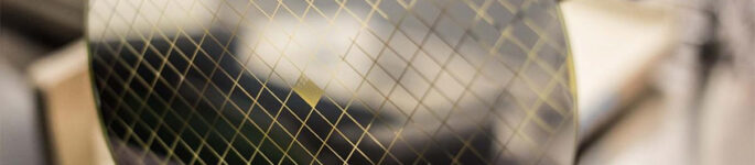
SILICON CARBIDE: FROM GOLD RUSH TO COMMODITY? By Stephen Rothrock (ATREG, Inc.), Jean-Christophe Eloy (Yole Group), and Poshun Chiu (Yole Intelligence, part of Yole Group) The extraordinary ascent of the
More »
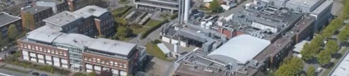
ATREG REPRESENTS ELMOS IN SALE OF 200MM DORTMUND FAB TO LITTELFUSE ATREG is pleased to announce that it has successfully advised Elmos Semiconductor SE on the sale of its 200mm
More »
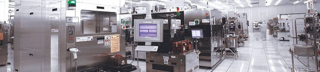
NEXPERIA ENGAGES ATREG REGARDING 200MM FAB IN NEWPORT, WALES, UK ATREG looks forward to working with Nexperia regarding its operational, automotive-qualified 200mm manufacturing facility located in Newport, South Wales, which
More »