


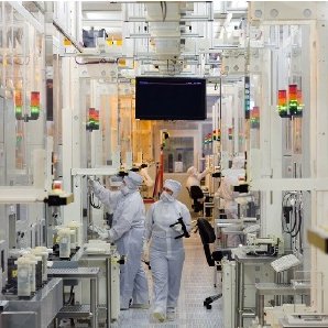
NEXPERIA ENGAGES ATREG REGARDING 200MM FAB IN NEWPORT, WALES, UK
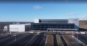
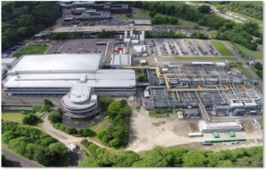 ATREG looks forward to working with Nexperia regarding its operational, automotive-qualified 200mm manufacturing facility located in Newport, South Wales, which is the UK’s largest semiconductor site spanning 28 acres (12 hectares). The campus features a 200mm ballroom cleanroom facility built in 1998, as well as a test area. It also includes a unique, former 150mm facility that could be used as a flexible modular cleanroom space. The facility is part of the South Wales Cluster, one of the top five semiconductor clusters in Europe with a well-established supply chain. With proper investments, the site can also be used for production of compound semiconductors. ATREG is excited to partner with Nexperia on this project following the successful close of other European fab assignments, including onsemi’s 150mm facility in Belgium and Texas Instrument’s 150/200mm facility in Scotland.
ATREG FACILITATES SALE OF LARGE OPERATIONAL JDI HIGASHIURA FAB TO SONY
ATREG is pleased to announce that it has facilitated the divestment of Japan Display Inc. (JDI)’s operational LCD display panel manufacturing fab located in Higashiura, Japan to Sony Semiconductor Manufacturing Corporation (SCK). The transaction will close on April 1, 2024.
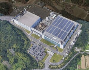 In May 2022, JDI announced that the company would end production at the Higashiura fab by March 2023 to increase JDI’s cost competitiveness and profitability, as stated in JDI’s earnings reports.
“Located on a 50-acre campus, the Higashiura fab features a total building area of over 1,000,000 sq. ft. as well as ballroom-type cleanrooms offering over 350,000 million sq. ft. of manufacturing space,” explains Stephen Rothrock, Founder, President, and CEO of ATREG. “While concerned about the size of the site and a short timeline to find and secure a buyer, ATREG nonetheless brought multiple interested parties to the table and through a competitive process allowed JDI to select the best buyer.”
“ATREG has been instrumental in helping us find the right buyer for our Higashiura manufacturing facility,” concludes Akihito Okochi, Chief Financial Officer of Japan Display Inc.
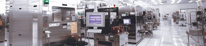
EXECUTIVE Q&A: MARCO CHISARI, EVP OF SSIC & HEAD OF U.S. FOUNDRY BUSINESS, SAMSUNG ELECTRONICS
![]() ATREG recently sat down with Marco Chisari, Executive Vice President, Head of SSIC (Samsung Semiconductor Innovation Center), and Head of U.S. Foundry Business in Samsung’s U.S. subsidiary, Samsung Semiconductor, Inc., to discuss the company’s current greenfield fab project in Taylor, TX, the U.S. CHIPS Act, and his latest industry insights.
ATREG recently sat down with Marco Chisari, Executive Vice President, Head of SSIC (Samsung Semiconductor Innovation Center), and Head of U.S. Foundry Business in Samsung’s U.S. subsidiary, Samsung Semiconductor, Inc., to discuss the company’s current greenfield fab project in Taylor, TX, the U.S. CHIPS Act, and his latest industry insights.
You have a long history in the semiconductor industry dating from the expansion of Mubadala to your investment banking career and now Head of Samsung’s U.S. Foundry Business. What are the most pressing concerns for the industry at present?
I came to Silicon Valley over 20 years ago to design flash memories. At that time, we were integrating the Flash with the first ARM controllers, ARM 7, and ARM 9 in system-in-package. About 25 years ago, I think we had Pentium 5, 3G in phones were still in their early stages, the NAND memory market was still small in size addressing mostly digital cameras, and the foundry industry was still in its very early innings. It is just extraordinary to reflect on how much has been achieved and accomplished by the industry in such a short period of time. As we all well know, the challenges have evolved very significantly.
To address the question in my personal view, the industry today has four key structural issues that need to be addressed:
1. The lack of investment in semiconductor start-ups and the limited access to capital for U.S. semiconductor start-up players
- The number of semiconductor start-ups, their growth, and financial capitalization are the closest proxy to predict the health and strength of the industry in the future
- While 2021 and 2022 have been remarkably positive years for VC investments in semiconductor, I personally do not see the trend to continue at that level in the coming years
- Innovation in AI, crypto, automotive, and power have been strong drivers, but still the numbers clearly indicate on average a reduction in the number of start-ups emerging across a broad spectrum of end-market applications
- More concernedly, this trend really applies to the U.S. and Europe. The number and the quality of semiconductor start-ups in China, on the other hand, is in rapid ascend and I believe that will have very significant repercussions on the structure of the industry in the next decade
 2. The excessive concentration of some key semiconductor technologies among just a few players
- This applies to the entire value chain – from semiconductor cap equipment, to EDA, to fabless players as well as foundry manufacturing players
- The waves of M&A consolidation in the last 15 years together with the reduction of emerging start-ups have driven player concentration in the industry
- Across the entire supply chain, many segments now have a sole supplier or just two large-scale suppliers
- I believe this creates intrinsic vulnerability in the supply chain and poses a structural risk to many customers and end-markets
3. The risk of bifurcation of the supply chain between China and the western world
- The current geopolitical tension and export control limitations are increasingly driving China to decouple their supply chain
- China’s long-term vision, their strong start-up ecosystem, and willingness to develop an independent domestic supply, in my opinion, in the short term will drive significant changes in supply allocation and an increasing domestication of Chinese semiconductor components in consumer electronics, PCs, and smartphone devices
4. The excessive dependency of the industry, particularly at leading edge, on Taiwanese suppliers and the vulnerability that creates for the industry and the overall economy
- As China has clearly stated their goal for national reunification, the excessive dependency on Taiwanese suppliers represents a clear single point of failure for the entire industry.
Can you provide us with an update on your greenfield fab plans in Taylor, TX?
 I am very excited about the Samsung foundry greenfield project in the USA. While some other players have made big statements, Samsung has worked quietly and diligently to the construction of its new leading-edge facilities in Taylor, TX, just 15 miles northeast of Austin. It is a very large-scale project – we have levelled 12,000 acres of land in March 2022, and since then have completed the foundation work for the first two fabs. The first fab structure is now under construction and the sheer size of the project is quite remarkable. The first two fabs will cover an area over half a mile long (about 900mm), but the site size will allow to host up to 10 fabs, including potentially R&D and packaging facilities if customer demand requires. We aim to complete the construction of the first fab shell by mid-year, and then we will start moving in the first tools. Manufacturing will start in late 2024, with the first wafers out before the end of 2024.
Why did you select this site for your greenfield build?
I think this site in Taylor, TX was selected for multiple reasons. To begin with, it is extremely close to our existing fab campus in Austin (Fab S2) where we have today the largest foundry manufacturing facility in the U.S. The Austin fab, in fact, is capable of 100,000 wpm. From Austin in 2022, we have shipped almost exactly 1.2 million wafers, mostly at 14nm, both for logic, RF, and analog mixed signal applications. So being close to the Austin campus is a tremendous advantage because in the last 20 years in that area, we have established a strong and vibrant supplier ecosystem that supports every aspect of the foundry manufacturing process. In that area, we believe there is also high-quality human capital that will be critical to ramp up the new facilities. Taylor is also strategically positioned closed to an airport and to a railroad which is critical to supply hundreds of tons of construction material. In Taylor, we have also secured access to water and electricity which are critical to our ability to operate the facility and potentially expand to more fabs in the future, if required. We have used local contracts for the construction and most of the workforce on site is from Texas. The team is doing an exceptional work in building the largest fab site in the U.S.
What are some of the biggest challenges you’ve faced so far?
Clearly in a project of this scale, we have faced a lot of challenges. We have to remember we have just been through a global pandemic that, combined with the war in Eastern Europe, has created a massive inflationary pressure on all construction material costs. The increasing cost of semiconductor equipment tools and the lead time of the equipment are still big challenges to manage. But more than anything, I want to highlight the difficulty to convince U.S. fabless customers to manufacture in the U.S. There is no question U.S. fabless engineering teams focus exclusively on PPA and cost and ascribe still little to no value to the geopolitical risk of a concentrated supply in Taiwan. We are seeing a chance of mindset happening, but it is still a big challenge to face.
 How are you preparing for staff recruitment amid today’s skilled labor shortage?
Recruiting talent is certainly a critical challenge. We plan to rely on the talent we already have on our campus in Austin where we count on over 3,500 highly skilled professionals. We will count on our team in South Korea to support the process technology transfers, but we will also heavily rely on hiring new U.S. talent. In this respect, Austin is a great area for talent in semiconductor, with a very strong ecosystem that encompasses semiconductor equipment, fabless companies, materials, and advanced technology.
There was some talk in the fall of last year that Samsung was reportedly considering building a new chip manufacturing plant somewhere in Europe. Can you tell us a little bit more about those European plans?
At this stage, we are focused on the site in the U.S. We are thoughtfully looking at other options, including Europe, but we will consider which technologies are most appropriate for each different geography and local end-market needs.
During your presentation at this year’s ISS Conference, you made a reference to the fact that there are many trillions dollars of market value today running the risk of a “single point of failure.” Can you elaborate on that comment?
The key issue is that today, many trillion dollars of market value of technology companies depend exclusively, or almost exclusively, on supply from Taiwan. I do believe at some point Wall Street investors will start paying attention to this risk and looking at the values of companies on a risk-adjusted basis. I personally find extremely concerning that the boards of U.S. semiconductor companies are not actively addressing this risk and are not actively preparing to address it. The market failure is simply too big to consider, but unfortunately the industry is accepting this massive system risk without hedging it. To be fair, we all know this does not apply to foundry only, but to many other aspects of the supply chain. The issue with foundry is that it is the most complex, the most expensive, and the most time-consuming to prepare and to hedge for.
 The call for CHIPS Act funding applications just opened in Feb. Do you feel that $52 billion will be enough to enable the U.S. to boost chip capacity and regain world leadership?
I personally believe that $52 billion is a good start. More importantly, the debate has allowed the industry to reflect and pay attention to the risk of limited semiconductor supply onshore. There is no question that, over the very long term, the industry may require more support, but I personally believe that the stability and consistency of the support will be as important as its dollar amount.
If not, what else will the U.S. need in your opinion?
If I may share a prospective, I personally believe it is not sufficient to support the growth of on-shore supply alone. I think it is equally important to incentivize the demand to manufacture in the U.S. The industry needs to come to terms with what it may take to absorb the costs of manufacturing in the U.S. U.S fabless executives do not want to address this topic. Yet. Waiting until the transition may become a necessity will simply create too much risk for public shareholders. I believe U.S. semiconductor boards have the fiduciary duty to thoughtfully reflect on these risks and benefits.
As the Head of Samsung’s U.S. Foundry Business, what are most excited about the future?
There are so many things that excite me about the opportunity to grow the Samsung Foundry business in the U.S. First and foremost is the possibility to help support the geographical diversification of the semiconductor supply. But also, I believe it is an exceptional time to be part of this industry as we transition to Gate-All-Around transistor technology. The industry has exhausted the capabilities of FinFet and a new GAA era is in front of us. We are playing at the absolute limit of physics, pushing the transistor and system performance to the absolute limit, with the most complex manufacturing equipment in the world. We are also at the beginning of a big transition to a more common use of 3D advanced packaging for chiplet solutions. We will not succeed alone. We will need the help and support of an immense amount of partners, as well as a strong and vibrant ecosystem. The financial stakes are getting exceptionally high and I personally believe a more balanced and diversified supply will be a good and necessary outcome for the industry and the world.
About Marco Chisari
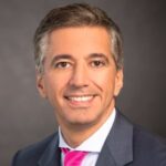 Marco is an Executive Vice President, Head of SSIC (Samsung Semiconductor Innovation Center), and Head of U.S. Foundry Business in Samsung’s U.S. subsidiary, Samsung Semiconductor, Inc. He has over 25 years of experience with global Fortune 500 organizations such as Bank of America Merrill Lynch, Credit Suisse, Mubadala, GlobalFoundries, JPMorgan, and STMicroelectronics where he developed his expertise in both investment banking and buyside, with particular focus on the semiconductor industry.
Most recently, Marco was a member of Bank of America Merrill Lynch as Managing Director, Global Head of Semiconductor and Mobility investment banking. In this role, he advised on different transactions, including the $35 billion acquisition of Xilinx by AMD, the $22 billion acquisition by Analog Devices of Maxim, the $9 billion sale of Intel NAND business to Hynix, the $10 billion acquisition of Cypress by Infineon, the $4.6 billion acquisition of Osram by AMS, Marvell acquisitions of Aquantia and Avera, as well a large number of debt financing, IPO, and equity-link transactions. Prior to BAML, Marco was Head of Mergers & Acquisitions at Credit Suisse in San Francisco and worked on a variety of semiconductor and software transactions. Before Credit Suisse, while at Mubadala, he contributed to the investment and formation of GlobalFoundries from its inception.
U.S. CHIPS ACT – WHO WILL BE THE BIG WINNERS?
By ATREG Founder, President & CEO Stephen Rothrock
 On February 28th, the U.S. Administration announced the long-awaited launch of the first funding opportunity for semiconductor manufacturing incentives since the passing of the bipartisan CHIPS Act last July. Of the $52 billion earmarked to revitalize the U.S. semiconductor manufacturing, $39 billion will be dedicated to incentives. All potential applicants are invited to submit statements of interest, so the U.S. Department of Commerce may begin application reviews. Funding awards will be made as soon as applications can be rigorously evaluated and negotiated. Click here for more details on the application process.
This first public funding opportunity seeks applications for projects to construct, expand, or modernize commercial facilities for the production of leading-edge, current-generation, and mature-node semiconductors, including both front-end wafer production and back-end packaging fabs. Awards will take the form of direct funding, federal loans, and/or federal guarantees of third-party loans. Awards are designed to complement – not replace – private investment and other sources of funding.
The timely CHIPS Act funding application process kicks in as the global semiconductor market is entering yet another downturn cycle this year. According to Malcolm Penn, Founder & CEO of UK industry analyst firm Future Horizons, the global chip market could contract by as much as 22% in 2023. In the U.S., greenfield fabs take two to four years from build to product qualification and we are still in the midst of an operational brownfield fab shortage that is likely to continue through to at least mid-2025. Given the huge cost of building highly advanced wafer fabs, the funding could go very fast amid fierce competition, so who will be the big winners?
 The companies that can execute a site selection process quickly – Case in point, Wolfspeed was one of the first U.S. companies to get on the incentives bandwagon in Mohawk Valley by selecting the Marcy Nanocenter near Utica, NY for its state-of-the-art 200mm silicon carbide fab that was inaugurated and started production in April 2022. Since then, other major chipmakers including Intel (OH), TSMC (AZ), IBM (NY), Samsung (TX), Micron (NY), and Texas Instruments (UT) have embarked on aggressive fab expansions to be able to claim some of that support in various U.S. states.
- The companies bringing capital to the table – The U.S. Administration does not plan to fund entire projects, but rather offer grants of between 5% to 15% of a company’s capital expenditures for a project, with funding not expected to exceed 35% of the cost. Companies can also apply for a tax credit reimbursing them for 25% of project construction. So far, more than $200 billion in private investments for U.S. semiconductor manufacturing projects have been committed since the CHIPS Act was signed into law.
- The companies committed to their local community– Those who will be creating hundreds of regional skilled jobs in a very tight labor market and will implement programs that will attract women into the semiconductor workforce, such as affordable, high-quality childcare, as well as training programs for local school, college, and university students.
 As part of the CHIPS Act funding program, at least two U.S. manufacturing clusters will be built to produce the most advanced types of logic chips, as well as facilities for other kinds of chips, and complex supply networks to support them. In light of where most greenfield builds are already happening, it is everyone’s educated guess as to which locations will be the lucky ones.
I think we can all agree that this initial public funding package will not be sufficient in the long term for the U.S. to regain its semiconductor manufacturing leadership on the global stage in light of fierce overseas competition. The U.S. needs to balance short-term investments that shore up capacity with spending aimed at mastering cutting-edge manufacturing, as well as longer-horizon R&D of next-generation technologies. Although one 2020 study found that a $50 billion investment in the semiconductor industry would increase U.S. market share to only 14%, this funding is the first necessary step towards kick-starting our U.S. onshore chip production efforts.
ATREG PRESENTED AT FOA’S 2023 COLLABORATIVE FORUM
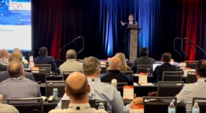 On February 23rd, ATREG Vice President Annie Rothrock was invited to speak at the Fab Owners’ Alliance annual Collaborative Forum held in Phoenix, AZ. Annie provided the latest overview of the U.S. semiconductor manufacturing asset market, supported by real-world fab transaction examples, touching on such topics as:
- The features / factors making brownfield fabs valuable
- The strategic benefits of selling and buying wafer fabs
- The challenges and recent market changes that fab sellers and buyers need to be aware of
- How new greenfield fabs coming online will affect U.S. semiconductor capacity
To request a copy of the presentation, please email Annie Rothrock.
![]() In case you missed it, catch up with our Founder, President & CEO Stephen Rothrock’s Viewpoint 2023 contributed column published in Semiconductor Packaging News on January 16th.
In case you missed it, catch up with our Founder, President & CEO Stephen Rothrock’s Viewpoint 2023 contributed column published in Semiconductor Packaging News on January 16th.
Fab sharing to increase in 2023
Pandemics, geopolitical tensions, energy crises, rising fab construction costs, endemic fab ecosystem issues, skilled labor shortages, and sustainability requirements are compelling global chip makers to find creative ways to deliver the capacity needed to meet global market demand while keeping manufacturing costs under control. As a result, fab sharing is slowly emerging as a new operating model we will likely see more of in 2023.
 Last July, STMicroelectronics and GlobalFoundries announced they were joined forces to create a new high-volume 300mm fab adjacent to ST’s existing 300mm facility in Crolles, France, supported by significant funding from the French government. This is not STMicroelectronics’ first fab sharing rodeo — the company is already operating its 300mm wafer fab in Agrate Brianza, Italy with Tower to accelerate analog and power semiconductor production.
In a world where total operational semiconductor capacity is currently provided by 153 300mm fabs, 223 200mm fabs, and 297 150mm fabs, operating existing 200mm brownfield fabs and mature nodes will remain critical for the future of our industry.
Core 200mm demand remains strong in light of the shortage of available 200mm fabs. With greenfield expansions mainly focused on 300mm leading edge, semiconductor manufacturers will still have to convert some 200mm fab tools to 300mm to keep up. As recessionary times lay ahead of us, fab sharing is a very smart move on behalf of chip makers to build on existing semiconductor clusters, share risks, and produce at a lower cost.
SEE YOU AT UPCOMING GLOBAL INDUSTRY EVENTS
 Will you be at any of the following global industry events over the coming months? If so, please don’t hesitate to email us to set up an appointment with one of ATREG’s fab transaction advisors to discuss your semiconductor infrastructure-rich manufacturing asset needs. We can assist your company with its global manufacturing strategy by helping you divest or acquire a brownfield facility or select the best location in the world for a greenfield build. We hope to see you there!
- JP Morgan Global Technology, Media & Communications Conference, May 22-24, Boston, USA
- Bank of America Merrill Lynch Global Technology Conference, June 6-8, San Francisco, USA
- SEMICON SE Asia, May 23-25, Penang, Malaysia
- GSA Global Leadership Summit, June 7, Tokyo, Japan
- GSA European Executive Forum, June 14-15, Munich, Germany
- SEMICON West, July 11-13, San Francisco, USA