



ATREG FACILITATES SALE OF ONSEMI’S PA FAB TO SILEX
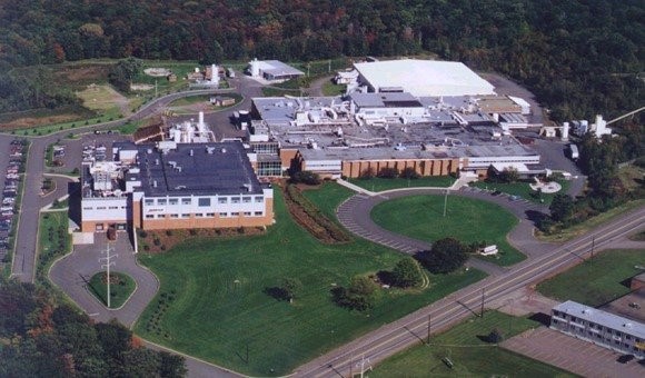 ATREG is pleased to announce that it has successfully assisted onsemi with the sale of its 200m operational fab located in Mountain Top, PA. onsemi has entered into an agreement with Swedish company Silex Microsystems to divest the fab as part of its ongoing strategic fab-right manufacturing model, which focuses resources on the most competitive, scalable, and technology-aligned operations worldwide.
The PA manufacturing asset is expected to change ownership in January 2028 subject to customary closing conditions and regulatory approvals. This time will allow onsemi to gradually transfer the products currently manufactured at the PA site to other facilities within its network, ensuring continuity for customers and a structured migration of technologies.

EUROPEAN 200MM CLEANROOM OPPORTUNITIES
 ATREG is currently actively advising on European cleanroom transactions across a range of asset scales, from large 200mm manufacturing campuses to smaller specialized environments, and has visibility into a growing pipeline of European cleanroom opportunities.
The European semiconductor cleanroom market is seeing a meaningful uptick in transaction activity, driven by the convergence of several themes. Demand from the AI infrastructure buildout, quantum computing commercialization, and a maturing start-up ecosystem are all meeting a steady stream of strategic divestitures from established IDMs. The result is a well-supplied opportunity landscape that ATREG views as one of the more active periods we have tracked in the European market over the past 25 years.
200mm: Still the backbone of industrial semiconductor manufacturing
Much of the public conversation around semiconductor investment centers on leading-edge nodes and 300mm capacity. The 200mm segment, however, remains the production backbone for analog, power, MEMS, sensors, and compound semiconductors. These device categories are central to EV powertrains, industrial automation, defense and aerospace electronics, as well as the emerging quantum hardware supply chain.
Europe has historically been a center of gravity for 200mm production, with established facilities across Germany, the Netherlands, Belgium, the UK, and other EU member states. As major IDMs continue to rationalize their fab footprints, a range of cleanroom assets are coming to market. These include large-scale, multi-building campuses with existing infrastructure and established workforces, as well as smaller, more specialized environments suited to research institutions, start-ups, or companies seeking a measured entry into the European manufacturing market. ATREG is currently engaged across both ends of that spectrum.
Why Europe, why now?
Having just released the Chips Act 2.0, European governments are competing aggressively for semiconductor capital. Recent commitments illustrate the scale of that ambition: Spain directed nearly $900 million in public funding toward Diamond Foundry’s synthetic diamond wafer facility in Extremadura, the Netherlands has mobilized over €1 billion through its PhotonDelta integrated photonics program, and the European Commission approved €128 million in state aid for X-Fab to build a new MEMS-focused open foundry in Erfurt, Germany.
Europe has historically been viewed as an expensive place to manufacture, but the current market is increasingly rewarding regions that combine a strong talent pipeline with generous government support. Add the strategic imperative many companies feel to diversify their supply chains away from Asia, and Europe has a credible and growing role to play in chip manufacturing this decade and beyond.
Should your company be currently evaluating European cleanroom acquisition or capacity partnership opportunities, please email ATREG Vice President Stuart Smith to discuss manufacturing assets currently available in the region and how these may align with your specific strategic objectives.
BEYOND IDMS AND FOUNDRIES: NEW CLEANROOM BUYERS ARE EMERGING
For most of ATREG’s 25-year history, the universe of cleanroom buyers has been relatively predictable – IDMs expanding capacity, foundries growing their footprint, the occasional private equity firm looking to monetize cleanroom assets. That picture is changing. ATREG has been closely engaged with the stakeholders driving this shift, and the range of organizations now evaluating cleanroom ownership or dedicated fab capacity is broader than at any point in our firm’s experience.
The vertical integration imperative: Tesla and Terafab
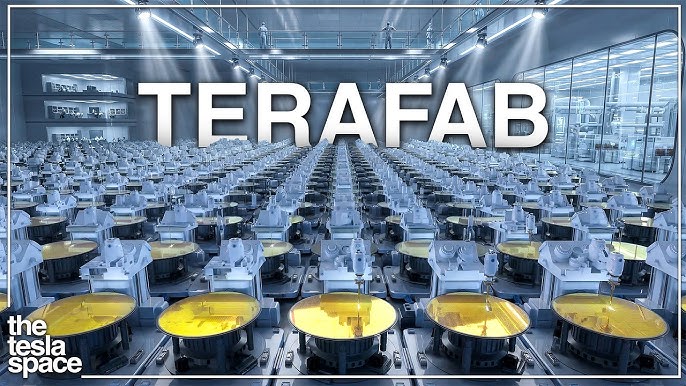
The clearest signal that something structural has changed came in March 2026, when Tesla and SpaceX jointly announced Terafab. Described as a vertically integrated, closed-loop facility spanning lithography, logic and memory fabrication, as well as advanced packaging, Terafab carries an estimated price tag of at least $55 billion and is sited at the existing Gigafactory Texas campus in Austin, TX. Elon Musk’s stated long-term ambition is one million wafer starts per month, producing between 100 and 200 billion custom AI and memory chips per year.
The strategic logic is hard to dismiss. AI compute demand has grown so extreme that a company of Tesla’s scale, with captive demand across vehicles, robotics, and the broader Musk business ecosystem, has concluded that dependency on external foundries is an unacceptable strategic risk. Whether Terafab succeeds or not, its announcement marks a new category of buyer entering the conversation: the large-scale technology company that has decided the cost of vertical integration is lower than the cost of supply chain dependency.
Quantum computing comes of age: IonQ, SkyWater, and the Commerce Department’s $2 billion signal
A quieter but arguably more significant development is the maturation of quantum computing as a cleanroom demand driver. Quantum hardware – particularly superconducting qubits – requires extraordinarily controlled fabrication environments, often more demanding than conventional semiconductor manufacturing. As the technology moves from research into commercial scale, the need for dedicated or semi-dedicated cleanroom capacity is growing.
In January 2026, IonQ announced an agreement to acquire SkyWater Technology, the largest exclusively U.S.-based pure-play semiconductor foundry, in a cash-and-stock deal valued at approximately $1.8 billion, with the explicit goal of creating the first vertically integrated full-stack quantum platform company.
The U.S. government has reinforced that signal at scale. On May 21, 2026, the Department of Commerce announced $2 billion in CHIPS Act incentives directed at nine quantum companies, supporting both domestic quantum foundries and quantum computing firms developing utility-scale, fault-tolerant systems. IBM received the largest allocation at $1 billion for a new dedicated quantum foundry, with GlobalFoundries receiving $375 million and companies including PsiQuantum, Rigetti, and Quantinuum each receiving up to $100 million. Structurally, this program is notable in that the government is taking a minority equity stake in each recipient, positioning Washington as a direct investor in quantum manufacturing infrastructure, not merely a grant-maker.
The policy message is clear: no major economy wants to fall behind in the race to commercialize quantum, and the infrastructure requirements of that race run directly through cleanroom capacity.
The start-up ecosystem and the VC-backed fab
A third demand driver is less visible, but increasingly real. A cohort of well-capitalized semiconductor start-ups – particularly in compound semiconductors, photonics, and power devices – has matured to the point where shared foundry access is no longer sufficient. These companies have developed proprietary processes that cannot be adequately supported by a merchant foundry model, and they are increasingly seeking either dedicated cleanroom space or the ability to acquire and operate their own facilities. Through our advisory work across both the U.S. and European markets, ATREG has seen this demand build steadily over the past two years.
On the horizon: Hyperscalers
 The category ATREG is watching most closely for the next wave of cleanroom interest is the hyperscalers. Google, Microsoft, Amazon, and Meta have each moved aggressively into custom silicon design, reducing their dependence on merchant AI chip suppliers. For now, these programs remain fabless – designed in house, manufactured at TSMC or through ASIC partners. But the strategic logic that drove Tesla toward Terafab applies to hyperscalers with equal or greater force. Their compute demand is larger, their capital position is stronger, and their tolerance for supply chain dependency is declining. ATREG anticipates that one or more hyperscalers will emerge as serious cleanroom buyers within this decade.
ATREG PARTICIPATES IN ENTEGRIS PANEL AT SEMICON EUROPA 2026
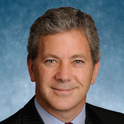 ATREG is pleased to announce that Founder & CEO Stephen Rothrock will participate in the Entegris executive panel discussion – Advanced Packaging: From Strategic Imperative to Scalable Reality in Europe – to be held on Wednesday, November 11th from 2:00 to 3:40 pm at this year’s SEMICON Europa in Munich, Germany (Executive Forum, Hall C1).
Moderated by Entegris, the panel discussion will bring together industry executives to share perspectives on key challenges and opportunities and explore how Europe can bridge the gap between innovation and industrialization, and secure advanced packaging as a cornerstone of future competitiveness.
Advanced semiconductor packaging has become a key driver of performance, integration, and competitiveness as front-end scaling reaches its limits – and a key differentiator. In Europe, advanced packaging is now a priority under the EU Chips Act, supporting ambitions for resilience, performance leadership, and sustainable growth.
Our sincere thanks to Entegris for their kind invitation! ATREG looks forward to seeing you all in Munich this fall!
Click here for more information on this SEMICON Europa session.
ATREG VIDEO INTERVIEW WITH SILICON SEMICONDUCTOR
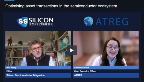 What drives value in semiconductor asset transactions — and what can go wrong without the right expertise?
In this video interview with UK publication Silicon Semiconductor, ATREG COO Annie Rothrock discusses what actually makes semiconductor asset transactions work, including the many factors that shape wafer fab dispositions and acquisitions — from cleanroom complexity to stakeholder alignment — and the kind of specialized expertise it takes to get deals across the finish line for both sides and deliver value for both buyers and sellers.
Click here to watch the full interview.
SEE YOU AT Q4 GLOBAL INDUSTRY EVENTS
 Members of the ATREG team will be back on the global semiconductor industry conferences circuit after the summer. Please feel free to email us to set up an appointment with one of our fab transaction advisors to discuss your specific infrastructure-rich semiconductor manufacturing asset needs, whether brownfield, greenfield, or capacity / loading partnerships. We look forward to seeing you there!
- ISIG Executive Summit EU, September 15-16, Prague, Czech Republic
- GSA U.S. Executive Forum, September 22, Menlo Park, USA
- SEMICON West, October 13-15, San Francisco, USA
- ITPC, November 1-4, Kapolei, USA
- SEMICON Europa, November 10-13, Munich, Germany
- GSA WISH Conference, November 10, Santa Clara, USA
- SIA Annual Awards Dinner, November 19, San Jose, USA
- GSA Annual Awards Dinner, December 10, Santa Clara, USA