


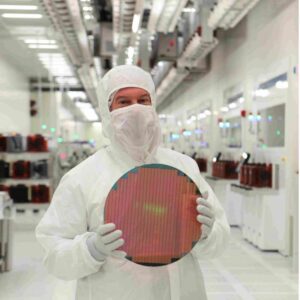
FEATURE ARTICLE: VETS AND SEMI – THE PERFECT MATCH
By Annie Rothrock, Vice President, ATREG, Inc.
 In the wake of the COVID pandemic, the chip shortage has wreaked havoc amid the global supply chain and disrupted production in many industry sectors, crippling the global economy for the past two years. In an attempt to address capacity constraints, governments everywhere have been offering attractive incentives to lure the world’s largest chip makers to their respective backyards to build new wafer fabs and create additional employment opportunities in their regions. But next to the chip shortage itself, a new issue is now on the mind of U.S. semiconductor manufacturers – skilled talent shortfall. With 13 to 15 new greenfield fabs in the pipeline in the United States alone between 2022 and 2025 needing an estimated 40,000 to 50,000 new skilled workers, how are we going to staff up those billion-dollar-plus facilities?
Last April, Wolfspeed’s Mohawk Valley silicon carbide fab was inaugurated following a joint $1 billion investment with the state of New York. Texas Instruments just broke ground on its new $30 billion manufacturing plant in Sherman, TX. Intel will invest more than $20 billion to build two new factories in Ohio. And TSMC was enticed into building a $12 billion fab in Arizona. In Europe, Intel is building a new €17 billion semiconductor manufacturing hub in Germany. In Asia, closed fabs even get a second life with Renesas reopening its 300mm Kofu factory (previously closed in October 2014) for the production of power semiconductors.
These days, workforce is even becoming a critical factor when acquiring a fab asset. It is no coincidence that Texas Instruments purchased Micron’s operational 300mm fab in Lehi, UT last year – an informed strategic move to also rehire all of the fab’s 1,215 employees as chip makers everywhere contend for skilled talent amid the labor shortage. So this begs the question: With time of the essence, what can the U.S. semiconductor industry do to quickly curb the skilled worker shortage over the short to medium term? Military veterans may provide the answer we are looking for. With nearly 200,000 service members leaving the U.S. military every year, there are many compelling reasons why semiconductor companies should look to vets as their next skilled hires.
SEMI: AN OPAQUE INDUSTRY
While other manufacturing industries in the U.S. such as aerospace have been successfully hiring vets for years, the semiconductor sector has been struggling to attract military personnel into its ranks for one main reason – a major lack of awareness of the industry among vets leaving service. Educating the microelectronics industry on the importance of tapping this critical demographic is only part of the equation. For an industry that is vital but often obscure to the general public, it is essential to create awareness of career opportunities amidst a fierce global competition for talent.
 Last November, the SEMI Foundation published a SEMI VetWorks Guide to help chip makers recruit and hire U.S. military veterans in addition to running an image and awareness campaign highlighting veterans with successful semiconductor careers. “What we as an industry need to show veterans is that they have the skills and ability to not only have a career in semiconductors, but to thrive and grow there,” explains Shari Liss, Executive Director at the SEMI Foundation. “Unless someone has had some exposure to the semiconductor industry, it’s not necessarily a go-to post-military career option. In addition, veterans may not recognize or consider the value that their experience can bring to the semiconductor workforce. Semiconductors are in the news now because of shortages, and because they are so critical to the economy and national security, the government is working to bring semiconductor manufacturing back to the U.S. That means more semiconductor jobs and additional job security. Service members can be part of the staffing solution.”
TRANSFERRABLE, MISSION-CRITICAL TALENT
As the largest pool of renewable skilled talent, U.S. military veterans are uniquely matched to the semiconductor industry, with skills transferrable to a semiconductor fab team. On the hard skills front, service members are trained to use and operate sophisticated, expensive equipment which they know how to maintain and repair (e.g. avionics, hydraulics, mechanics, and radio frequency). They are attentive to detail, are extremely safety conscious, and many already enjoy security clearances ensuring the safety of intellectual property. On the soft skills front, veterans possess a great work ethic and strong sense of team instilled in them during their military service, as well as personal accountability, leadership, discipline, and a can-do attitude.
“There are many compelling reasons to hire veterans, but there is one that we don’t necessarily think about – aiding diversity program issues over time,” explains Kathy Garner, Talent Acquisition and Global Mobility Senior Manager at TEL. “The military is a diverse group with 16% females and 44% people of color. Military personnel come from a wide variety of experiences – from across all 50 U.S. states with a variety of cultural and economic backgrounds. Some even have international experience from being stationed abroad and speak multiple languages. That global citizen aspect of vets can be a valuable asset for some companies.”
EARLY ADOPTERS
According to the Pew Research Center, 99.5% of the U.S. population has zero direct working experience with the military. Civilian employers do not understand what the military does, the technical nature and responsibility of each role, or the extensive training each military member receives. And on their side, veterans do not understand the civilian workspace, creating a gap translating military experiences and skills to the civilian workforce and vice versa.
 Yet a few early adopters are already bridging the gap and hopefully paving the way for others to follow in their footsteps, including Intel, EMD Electronics, Infineon, Micron, Samsung, Indium Corporation, GlobalFoundries, Applied Materials, Wolfspeed, and Tokyo Electron Ltd. (TEL) to name just a few. “Hiring veterans has always been a priority for us as part of our strategic plan and we truly understand the strategic value veterans bring to the workforce,” adds Garner. “Our U.S. leadership team is comprised of 20% prior military and our president is our top veteran representative committed to military outreach and hiring initiatives. Although this match does make perfect sense, military hiring requires a different approach, and for many companies, as well as service members and veterans, there remains a challenge interpreting military skills and job experience translation to job openings.”
U.S. STATES ARE MOBILIZING
For years, U.S. states have been ramping up various initiatives to develop talent pipelines, career pathways, and training initiatives aimed at boosting veteran employment in semiconductors. To date, the Manufacturing Institute’s Heroes MAKE America initiative has graduated participants from military installations in Kansas, Texas, North Carolina, Georgia, and Kentucky. Graduates represent 136 different military specialties with an average of 11.5 years in service. More than 47% of these graduates are from minority populations. The program has a 92% placement rate at more than 250 companies across 39 states since its launch in 2018.
Led by and located at the SUNY Polytechnic Institute in Albany, Upstate New York, NEATEC (Northeast Advanced Technological Education Center) is an ATE Regional Center funded by the National Science Foundation (NSF). NEATEC fulfills the needs of the nanotechnology and semiconductor manufacturing industries in New York State and Western New England by supporting the education and training of technicians. “We offer our Veteran Semiconductor Training and Experience Program (Vet S.T.E.P.) at no charge to the military community over a period of 10 weeks – two weeks of hands-on advanced manufacturing training at our Nano Tech Center and eight weeks of industry internship with a choice of several industry partners. This Career Skills Program approved by the Army is the first of its kind in the country,” explains NEATEC Associate Director Kate Alcott. “But more importantly, our outreach educates service members about employment opportunities available in semiconductors and demonstrates the transferability of military training and discipline to the microelectronics manufacturing field.”
In a press release earlier this year, New York’s Governor Kathy Hochul declared “In New York, we are deeply committed to supporting the brave men and women who serve and protect our country, and we are forever thankful for their service. Today, we reaffirm our commitment to New York’s service members with concrete action, and the new Vet S.T.E.P. program is the latest example of our workforce initiatives focused on helping veterans find meaningful, long-term employment after leaving the military. This new program will serve as a model for the rest of the nation to follow, and will put veterans on the path toward a successful career while strengthening the U.S. semiconductor industry.”
 In Pennsylvania, the Penn State Center for Nanotechnology Education and Utilization (CNEU) has been providing the microelectronics/nanotechnology industry with trained workers from technicians to research scientists since 1998. The Nanofabrication Manufacturing Technology (NMT) partnership (between Penn State University and associate and baccalaureate institutions) across Pennsylvania has trained 1,000 community college and university students so far via its 18-credit hands-on capstone semester. “CNEU will be taking its military focused program national with locations in Atlanta, Phoenix, San Diego, and Norfolk in order to expand the Nanotechnology Certificate Program for active-duty military and veterans across the country in the coming years,” explains Robert Ehrmann, CNEU’s recently retired Managing Director. “Penn State’s CNEU and eight post-secondary institutions across these four locations have formed the Microelectronics and Nanomanufacturing for Veterans Partnership (MNVP) that will include various associate- and baccalaureate-level institutions. The MNVP is set to begin in September 2022 with classes for active-duty military and veterans beginning in 2023.”
Things are moving in many other states as well. Last March, Intel announced that it would place a priority on hiring military veterans when it begins to fill thousands of new jobs for its incoming plants in Ohio. In May, the SEMI Foundation was awarded a $1.5 million grant to bolster Michigan’s semiconductor industry talent pipeline. And in veteran-rich states like Texas, local companies such as Samsung are already committed to hiring vets, which will build a $17 billion semiconductor factory just outside of Austin.
MOVING FORWARD
Industry, academia, trade associations, and experts in the U.S. agree across the board – that there is still a long way to go, both at federal and state levels. But the good news is that President Joe Biden officially signed the CHIPS and Science Act into law by on August 9th – a monumental legislative win for the U.S. semiconductor industry. The bill provides a 25% tax credit for U.S. facilities that produce semiconductors or chipmaking equipment and $52 billion in funding for new semiconductor programs. The funding includes $39 billion for grants available to semiconductor manufacturers as well as equipment and materials suppliers and $11 billion for federal semiconductor research programs.
“I am hopeful that the U.S. government will start collaborating more closely with semiconductor industry associations representing well over 2,400 companies in the semiconductor supply chain,” explains Alcott. “This would help fast track the message to military members that the semiconductor industry offers lucrative jobs and stable career growth. Messaging to perspective employers highlighting the valuable skills veterans bring to their workforce should encourage more career development programs such as Vet S.T.E.P.”
 “This labor shortage was predictable given the explosion in technology we’ve been experiencing over the past 25 years,” comments CNEU’s new Managing Director Dr. Zachary Gray. “Industry as well as government must be willing to provide reputable academic institutions preparing today’s and tomorrow’s workforce with sustainable funding to supply a trained workforce for them in the boon as well as inevitable economic downturns. Without the sustainable funding of academic institutions, we are unable to support the faculty as well as the high-technology equipment and requisite maintenance costs needed to sustain these cutting-edge programs for our vets.”
“It is important for both employers and workers to know that working in semiconductors supports U.S. national and economic security,” says Liss. “Part of our work is to collaborate with the industry to provide support for veteran training that will make the transition more seamless. The job “crosswalks” that the SEMI Foundation has built into our career portal are one facet of this, and will help veterans better understand how their skills translate to the industry. Transitioning from the military to a civilian career can be overwhelming and challenging to navigate. At the top of our wish list is a one-stop shop where veterans could easily plug in their military occupational specialties (MOS) and connect directly to job openings in the semiconductor industry. This would alleviate decision fatigue and make the choices easier.”
“Employers, military transition teams, and veterans would greatly benefit from a well-marketed clearing house type of platform,” concludes Garner. “This platform would incorporate recruiting, marketing, and technology strategies to accomplish several key aspects – a vetting process of potential employers prior to platform access ensuring they inherently have military veterans’ best interest at heart; clean, easy-to-read templates for participating employers to advocate for themselves as military friendly employers with career opportunities, and most importantly matching military veterans to potential careers choices that best fit their interest and backgrounds. For now, many employers have a difficult time making first contact with the military transition teams due to a lack of contact information. Military transition teams do not necessarily feel comfortable sharing access to military members if the company is an unknown – this is where the importance of vetting comes into play. To overcome this, I recommend reaching out to those of us who already have military hiring programs. Many of us who are passionate about hiring and retaining veterans would be willing to share our experience to help set up your vet recruiting and hiring program.”
NEW YORK BEST-POSITIONED STATE FOR CHIPS ACT FUNDING
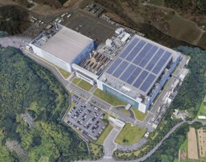
 The long-awaited CHIPS Act is here and the question now is – who gets a share of the $52 billion pie? With so many greenfield fab builds planned over the next couple of years on U.S. soil, how can chip makers wishing to take advantage of the benefits of the U.S. CHIPS Act funding best position themselves? To the winner goes the spoils – companies that can execute a site selection process quickly for either a new greenfield or existing wafer fab will come out on top. The best greenfield U.S. success story we have to illustrate this is Wolfspeed’s Mohawk Valley fab. As the most recent facility built in the U.S., their new 200mm SiC fab is the perfect example of how beneficial a precise wafer fab/cleanroom selection process can be ($1.3 billion investment, two-year construction, 600+ jobs).
Wolfspeed’s fab was built on the Marcy Nanocenter site near Utica in Upstate New York, the most shovel-ready site of any of the available greenfield sites in the U.S., making it ideally positioned for CHIPS Act funding investment. New York State is leading the way by offering a state-level, companion incentive to the federal CHIPS incentives. By recently passing its Green CHIPS Program – up to $10 billion in economic incentives for environmentally friendly green chips semiconductor manufacturing and supply chain projects, NY will reduce the cost of constructing and operating chip fabs. This new transformative program will help attract thousands of jobs and billions of dollars to cement New York as the nation’s leader in the domestic reshoring of semiconductor manufacturing—all while helping address supply chain shortages, inflation and national security.
Please email ATREG Vice President Annie Rothrock for more information on the Marcy Nanocenter shovel-ready site near Utica, NY.
AVAILABLE FOR SALE: JDI OPERATIONAL FAB, HIGASHIURA, JAPAN
 Japan Display, Inc. (JDI) has exclusively retained ATREG to help with the sale of its operational LCD G3.5 fab located in Higashiura, Aichi Prefecture. Built out in 1998 (F-Tower and Energy Tower) and 2002 (C-Tower), the fab currently manufactures various display technologies (DSC, wearable, mobile, VR, and HUD) for multiple industries, including automotive. Easily accessible via Chubu International Airport, rail, and ports, this facility could easily be converted to accommodate data center use, semiconductor manufacturing, or other high-technology production, such as battery, solar, medical devices, or pharmaceutical. This fab is a unique opportunity for a company that requires well-designed, infrastructure-rich advanced manufacturing space. Certain LCD tools are also available for purchase as a separate asset sale.
Offering highlights
- Total site area – 85 acres (201,774 m2)
- Total building area – 1,280,905 ft2 (119,000 m2) (three-building connected campus with five separate cleanrooms located in two buildings)
- Cleanrooms – Ballroom type offering 387,673 ft2 (36,016 m2) of manufacturing space
- Operating line specification – 5 glass substrate (600 × 720 mm) for small LCD panels (digital cameras / wearable devices)
- Certifications / ratings – IATF 16949 (automotive management system) and ISO 14001 (environmental management system)
- Available power – Up to 52MW
For further information on this offering, please email ATREG’s Senior Associate Tom Johnson.
SAVE THE DATE: NOVEMBER 17 PANEL DISCUSSION, SEMICON EUROPA
ATREG is pleased to announce that it has been invited to lead a special semiconductor manufacturing session at this year’s SEMICON Europa in Munich, Germany. The session entitled Greenfield vs. brownfield – how global government incentives could tip the fab balance will take place in the conference’s TechARENA in Hall C1, from 13:30 to 14:30 pm on Thursday, November 17th.
 The session will start with a 20-minute overview of the world’s semiconductor manufacturing asset market followed by a panel moderated by ATREG Founder, President & CEO Stephen Rothrock. The panel will feature experienced strategic operational executives from global semiconductor companies who will each share their own company’s manufacturing experiences, including:
- Alexander Gorski, Executive Vice President, Back-End Operations, Infineon Technologies AG
- Dr. Patrick Leinenbach, Senior Vice President, Automotive Electronics, Robert Bosch GmbH
- Abdelkarim Moharram, Manager, Business Development, Semiconductors, Manufacturing & Technology, Bethtel Corporation
- Rudi De Winter, CEO & Managing Director, X-FAB
The panel will discuss how global government incentives could tip the balance between greenfield fab builds versus existing brownfield fabs to meet the chip capacity that the world needs. Greenfield fabs take two to three years to build with an additional two years to install tools and qualify product. The key questions we’ll try to answer are: Will government incentives be enough to support the global greenfield fab construction effort? Could adapting current available brownfield fabs with new tools be a faster and more affordable alternative amid the current geopolitical and economic climate?
We hope you can join us! Access to the panel is complimentary for all SEMICON Europa and electronica show floor visitors. Click here to register for the event.

KEY TAKEAWAYS FROM MCKINSEY’S T-30 CEO SUMMIT
ATREG Founder, President & CEO Stephen Rothrock was invited to attend McKinsey & Company‘s T-30 CEO Summit that took place from September 21st to 23rd in California, along with executives from the world’s top semiconductor companies.
Since 2011, the event has convened leaders from the semiconductor, industrial, and technology ecosystems to discuss high-priority topics shaping the semiconductor and industrial-tech sectors, including leading business executives, academicians, investors, as well as start-up founders and innovators.
Here are a few of the key challenges identified from this year’s event as the group looked to how the industry would achieve $1 trillion by 2030 :
- Unprecedented capacity build-out is happening, leading to labor and equipment shortages
- Geopolitical tensions and the driving need for increased supply chain resilience
- Sustainability expectations from customer and investor stakeholders
- Fab ownership, mature product technologies, growing technology complexity, and R&D costs for leading-edge
 ATREG Founder, President & CEO Stephen Rothrock was recently interviewed by law360.com about the state of U.S. semiconductor manufacturing. The article entitled Is U.S. Industrial Real Estate Ready For A Chip Boom? penned by Senior Real Estate Reporter Valentina Pasquali was published on July 27th.
Click here to read the full article.
Click here to follow Stephen’s regular global semiconductor industry insights on LinkedIn.
CONNECT WITH US AT UPCOMING GLOBAL INDUSTRY EVENTS
 Busy travel times ahead for the remainder of this year for the ATREG team! We look forward to connecting with you at one of the following global industry events to discuss your semiconductor infrastructure-rich manufacturing asset needs. Please email us should you wish to set up an appointment with one of our fab transaction advisors. See you there!
- MEMS & Sensors Executive Congress, October 10-12, Coronado, USA
- FOA Q4 Members Meeting, October 26-27, Kissimmee, USA
- International Trade Partners Conference (ITPC), October 30 – November 2, Kohala Coast, USA
- SEMICON Europa, November 15-18, Munich, Germany
- SIA Annual Awards Dinner, November 17, San Jose, USA
- GSA Annual Awards Dinner, December 8, Santa Clara, USA