


ATREG FACILITATES GLOBALFOUNDRIES’ 300MM NY FAB SALE TO ON SEMI
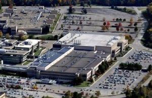
ATREG announced today that it has successfully represented and assisted ON Semiconductor Corporation with the structure of a transaction to acquire GLOBALFOUNDRIES’ 300mm fab located in East Fishkill, New York for an amount of $430 million. Under the terms of this phased purchase agreement, $100 million was paid at signing and $330 million will be paid at the end of 2022, at which point ON Semiconductor will gain full operational control of the fab and the site’s workforce will fully transition to ON Semiconductor. GLOBALFOUNDRIES will manufacture 300mm wafers for ON Semiconductor until the end of 2022, with the first production of 300mm wafers for ON Semiconductor expected to begin in 2020.
 The transaction also includes a technology transfer and development agreement as well as a technology license agreement, enabling ON Semiconductor to convert its wafer processes from 200mm to 300mm and to have immediate access to advanced CMOS capability, including 45nm and 65nm technology nodes.
“The ATREG team provided key insight in bringing this partnership together,” explains Keith Jackson, President and CEO of ON Semiconductor. “This will allow us to intensify our investments in the differentiated technologies that fuel our growth while securing a long-term future for the Fab 10 facility and our employees.”
“This transformational transaction is a win-win-win outcome for all stakeholders involved,” adds Stephen Rothrock, President and CEO of ATREG. “ON Semiconductor accomplishes another major milestone in securing its leadership in power and analog semiconductors, GLOBALFOUNDRIES can further optimize its manufacturing assets globally by transitioning its numerous technologies to the company’s three other at-scale 300mm sites, and the Mid-Hudson Region will keep high-paying manufacturing jobs in New York State.”
For more information on this transaction, please email Nick Papa.
ATREG HELPS VIS ACQUIRE GLOBALFOUNDRIES’ 200MM SINGAPORE FAB
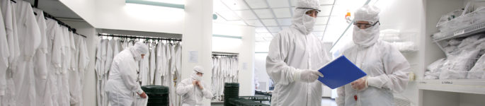
ATREG has successfully advised Vanguard International Semiconductor Corporation (VIS) on the acquisition of GLOBALFOUNDRIES’ operational 200mm Fab 3E located in Tampines, Singapore. The transaction, which amounts to USD$236 million, includes buildings, facilities, and equipment, as well as the intellectual property associated with GLOBALFOUNDRIES’ MEMS business. Under the terms of the supply agreement, the fab which currently offers a capacity of approximately 35,000 eight-inch wafers per month is expected to produce more than 400,000 per year. GLOBALFOUNDRIES (GF) will continue to operate the facility until the end of 2019 which will provide a transition period to facilitate technology transfers for VIS and existing GF customers. VIS will transfer all of Fab 3E’s employees to ensure there is no disruption to customers whose products are currently in production at the fab.
 “We had been looking for a 200mm facility that could meet our needs for extra capacity,” explains Leuh Fang, Chairman of VIS. “ATREG assisted us and leveraged their deep knowledge of the market to locate and work with us to secure this unique asset at a time when 200mm fabs are in limited supply. Together with the ATREG team, VIS are pleased to have negotiated this 200mm deal with GF for a win-win outcome.”
“This transaction is the result of diligent work with VIS’ relentless management team and ATREG could not be more pleased about the outcome for both parties involved,” adds Stephen Rothrock, President and CEO of ATREG. “The 200mm fab will be very beneficial in extending VIS’ manufacturing and product portfolio. In addition to VIS picking up a very qualified workforce, this new Singapore fab becomes their first facility outside Taiwan and further extends their reach and capability.”
For more information on this transaction, please email Nick Papa or click here to read the GLOBALFOUNDRIES press release.
ATREG ASSISTS TEXAS INSTRUMENTS WITH 200MM UK FAB SALE TO DIODES
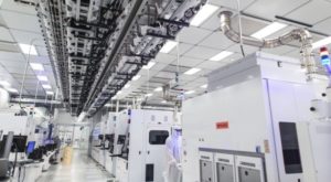
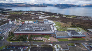
The ATREG team is pleased to share that it has successfully advised Texas Instruments (TI) on the sale of its operational 200mm / 150 mm wafer fab located in Greenock in Scotland, UK (GFAB) to Diodes Incorporated. Diodes will integrate the Greenock facility and fab operations into its fold, including retaining all GFAB employees. As part of a multi-year wafer supply agreement, Diodes will continue to manufacture TI’s analog products from GFAB as TI transfers into its other fabs. GFAB will offers Diodes additional wafer fab capacity to support its product growth, in particular its automotive expansion initiatives, as well as excellent engineering skills and wafer fab know-how to support its technical and operational performance expectations. TI’s 318,782-sq. ft. facility has a potential capacity of up to 21,666 wafer starts or 256,000 eight-inch equivalent layers per month, depending on product mix.
 “We have entrusted ATREG with multiple fab dispositions over the years, so we knew we could trust the team to also find the right buyer for our Scottish fab,” explains Kyle Flessner, Vice President of Worldwide Manufacturing Operations for Texas Instruments. “We appreciate their professionalism, persistence, and ability to work closely with us and Diodes to conclude a successful transaction.”
“It has been a long journey since the project first kicked off in 2016, but our tenacious global marketing effort allowed us to come to a viable deal that meets TI’s needs and offers Diodes a suitable supply agreement and product transfer,” adds Stephen Rothrock, President and CEO of ATREG. “Our thanks to the TI management team, the Scottish government, Scottish Development International, and Inverclyde Council for their assistance along the way in enabling the entire TI workforce to be kept in place.”
For more information on this transaction, please email Annie Rothrock or click here to read the Diodes press release.
VIEWPOINT 2019
By Stephen Rothrock, President & CEO, ATREG, Inc.
Originally published in Semiconductor Packaging News on February 4, 2019
Despite the industry’s optimistic growth forecasts, global uncertainty generated by trade wars is compelling advanced technology companies to constantly rethink their manufacturing strategies. In 2019, infrastructure-rich cleanroom manufacturing assets are going to continue to play an essential part in shaping these strategies to ensure global competitive advantage as more wafers are needed and more facilities are being built worldwide, e.g. in China or Intel’s $11 billion expansion in Israel.
 Whether to divest or acquire, go brownfield or greenfield, ATREG has helped some of the world’s largest and most reputable companies in the disposition and acquisition of back-end fabs and cleanrooms over the past 20 years. In the last year and a half alone, this includes the disposition of Micron’s Akita, Japan assembly and test plant to Taiwanese Powertech Technology (PTI) or the disposition of Qualcomm MEMS Technologies’ Longtan, Taiwan display facility to TSMC who converted it into an advanced packaging production plant.
In 2018, ATREG worked on more buy-side assignments than ever, witnessing increased interest in U.S.-based manufacturing as well as a continued lack of 200mm and 300mm capacity. And we should not expect 2019 to be any different. Despite a slowdown in semiconductor M&A activity, the global semiconductor market will continue to consolidate as the manufacturing needs of companies evolve with market changes. This has put a strain on manufacturing space and resulted in a number of new capital projects and expansions that may become difficult to fulfill in the current market.
A shortage of existing manufacturing space means cleanrooms and operational fabs will sell at a premium. Many companies are also looking at greenfield sites with Government incentives playing an active role. Running in tandem, there is still a shortage of used and new production tools with lead times in excess of one year to purchase new fabs from OEMs or equip new fabs.
For questions or more information, please don’t hesitate to email Stephen directly.
SEE YOU AT GLOBAL INDUSTRY EVENTS!
 Members of the ATREG team will attend several global industry conferences over the coming weeks. Please email us to set up an appointment with one of our experts at those events to discuss your specific infrastructure-rich manufacturing asset needs, including cleanrooms, fabs, and secondary tools.
- JP Morgan’s Global Tech, Media & Communications Conference, May 14-16, Boston, USA
- Bank of America Merrill Lynch’s Global Technology Conference, June 4-6, San Francisco, USA
- Stifel’s Cross-Sector Insight Conference, June 10-12, Boston, USA
- GSA’s Silicon Summit, June 18, Santa Clara, USA
- SEMICON West, July 9-11, San Francisco, USA
We look forward to connecting with you there!