
AVAILABLE FOR SALE: ON SEMICONDUCTOR OPERATIONAL 150MM FAB, OUDENAARDE, BELGIUM
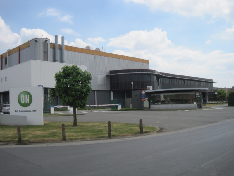
ON Semiconductor (Nasdaq: ON) has hired ATREG to find a buyer for its operational, automotive-qualified manufacturing facility located in Oudenaarde, Belgium, one hour’s drive from Brussels. The company is looking for strategic partners willing to enter into a mutually beneficial arrangement that will facilitate an orderly transition of products from the Oudenaarde fab to other ON Semiconductor facilities. This fab was acquired from AMI Semiconductor in 2008. The opportunity includes a high-end, fully integrated line of 200mm-convertible, 150mm tools capable of manufacturing 19,000 wafers per month down to 0.35 μm.
OFFERING HIGHLIGHTS
-
 Location – Close proximity to the world’s leading innovation and manufacturing hub in a stable region with a strong semiconductor ecosystem and extensive automotive presence
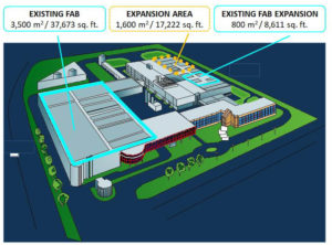
 - Cleanroom – 4,300 m2 / 46,284 sq. ft. of cleanroom space located on a 10-acre campus
- Supply agreement – Potential for immediate, sustained cash flow with multi-year supply agreement with ON Semiconductor
- Tools – 250 front-end manufacturing tools, approx. 80% of which are convertible to 200mm
- Products – 0.35 μm to 2 µm low-, medium-, and high-voltage analog CMOS and BCD technologies
- Workforce – Team of 400 highly motivated and skilled employees with extensive experience managing a diverse array of technologies, including an experienced management team, 200 operators, 95 technicians, and 50 engineers
This facility is an attractive asset for any global semiconductor company looking for a manufacturing foothold in Europe. For more details on this offering, please email Nick Papa, ATREG’s Vice President, Client Services.
CREE | WOLFSPEED FAB CONSTRUCTION STARTS IN NY / 434 ACRES WITH ONE MILLION SQ. FT. CLEANROOM SPACE STILL AVAILABLE AT MARCY NANOCENTER
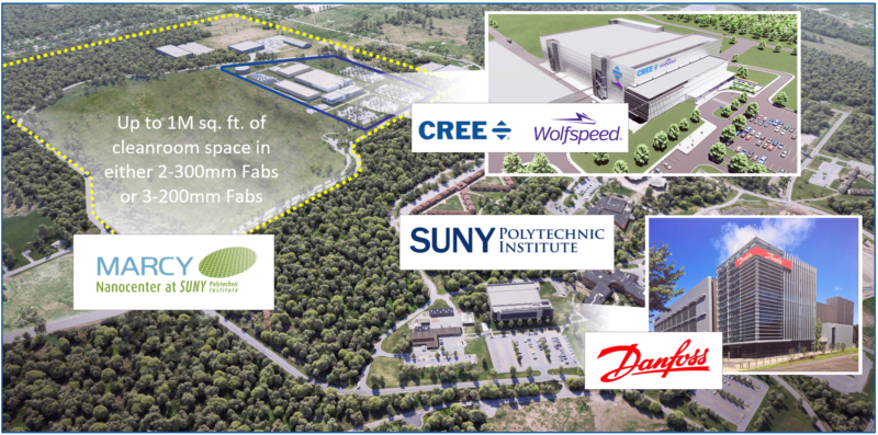
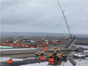 Since our last update in December 2019, Cree | Wolfspeed has hit the ground running with the construction of its new, leading-edge 200mm-capable silicon carbide (SiC) greenfield fab located at the Marcy Nanocenter near Utica in Upstate New York.
JBS Dirt, Inc. has now completed the excavation part of the site project and is now preparing the land for construction. The foundation and steel orders have been submitted and Exyte U.S.’s site plans have been approved.
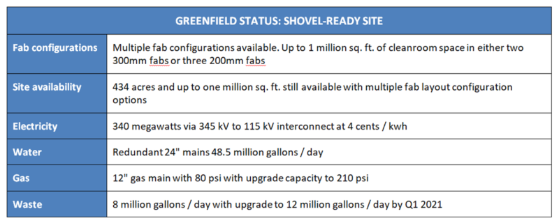
Two tiers amounting to one million sq. ft. of cleanroom space are still available close to the Cree fab for additional fab construction, as illustrated in the diagram below:
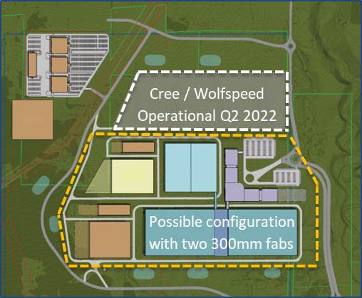
The Cree fab foundation work is expected to start in spring 2020. Tool installation is scheduled for April 2021 after which the cleanroom will be tested. Until then, Cree | Wolfspeed will have use of the Albany SUNY Poly cleanroom and plans to continue development work there while starting work in Marcy. With much of the company’s growth expected to be driven by the electric vehicle market, there is room to construct a second cleanroom space at a later stage, expanding the original fab to accommodate increasing market demand.
WORKFORCE
Cree | Wolfspeed has not wasted any time when it comes to hiring. At least 614 jobs are expected to be created over the next eight years and hiring has already actively started in Albany as well as Marcy. When the plant becomes fully operational in Q2 2022, employees will work across four shifts. Job openings range from leadership and engineering roles all the way to manufacturing and equipment technicians. Click here for a list of all Mohawk Valley fab-related job openings in Albany and Marcy.
ESTABLISHED SEMICONDUCTOR ECOSYSTEM
- Known for its technology leadership and innovation, Upstate New York has an established and growing semiconductor fab base, including facilities owned by GLOBALFOUNDRIES, Rohm, ON Semiconductor, and now Cree | Wolfspeed.
- Equipment and consumables suppliers in the region include KLA-Tencor, LAM, AMAT, ASML, TEL, Air Liquide, and Dupont, among others. Additionally, many suppliers have expressed interest in co-locating at Marcy Nanocenter as appropriate.
- The U.S. Bureau of Labor Statistics projects an 8.8% increase in STEM occupations through 2028.
- The region offers over 900,000 sq. ft. of cleanroom space.
- The region employs roughly 11,000 semiconductor industry / R&D professionals and produces over 5,500 STEM graduates per year from distinguished four-year universities such as Cornell, Rensselaer Polytechnic Institute (RPI), Rochester Institute of Technology (RIT), Clarkson, the University of Rochester, as well as SUNY at Binghamton, Albany, and Buffalo.
FOR MORE INFORMATION
Should your company wish to inquire about greenfield fab opportunities next to Cree | Wolfspeed at the Marcy Nanocenter near Utica, NY, please email Annie Rothrock, ATREG’s Director of Business Operations.
AVAILABLE FOR SALE: ALLEGRO MICROSYSTEMS CLEANROOM, SARABURI PROVINCE, THAILAND
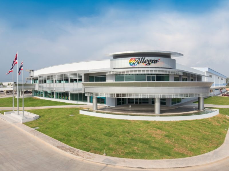
Allegro MicroSystems has retained ATREG to facilitate the sale of its production-ready, state-of-the-art cleanroom facility located in Saraburi Province, north of Bangkok, Thailand. Originally used for the assembly and testing of power IC products for the automotive industry, this manufacturing asset can accommodate the needs of multiple advanced technology sectors requiring a cleanroom environment. The 19.38-acre site consists of a 34,115 m2 (367,078 sq. ft.) facility with cleanroom production areas, production support areas, office space, and unimproved shell space. As part of the campus, there is 30,692 m2 (7.58 acres) of developable land adjacent to the facility ready for future expansion that could effectively double the manufacturing capacity of the site.
OFFERING HIGHLIGHTS
 State-of-the-art facility – A pristine automotive-qualified fab built in 2015
- Flexibility – The facility can be adapted to support the production of various advanced technology devices in addition to semiconductor A&T, including battery production, LED, medical devices, etc.
- Expansion potential – Ability to expand footprint on 7.58 acres of land adjacent to the existing facility
- Price – Opportunity to acquire a state-of-the-art cleanroom facility at a price below replacement value
- Location – Stable, cost-effective manufacturing region with a strong electronics supply chain / ecosystem and secure IP environment; located outside the 2011 flood zone and raised 8.4 meters (27.5 feet) above mean sea level, the facility is hardened against flooding
- Workforce – Access to highly skilled workers experienced in semiconductor A&T manufacturing
This offering is an attractive opportunity for a global advanced technology manufacturing company looking for a cleanroom in the Asia-Pacific region. For more details on this facility, please email Nick Papa, ATREG’s Vice President, Client Services.
ATREG ANNOUNCES TWO NEW HIRES
We are happy to welcome two new members to the ATREG team this year.
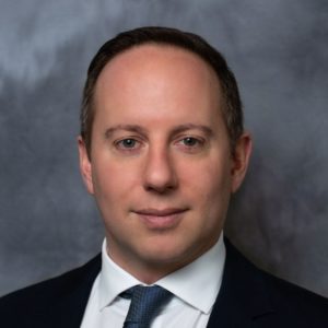 Tom Johnson joins ATREG as Senior Associate, bringing 18 years of telecom industry experience to the company. He is responsible for sourcing, executing, and managing the day-to-day operational aspects of multiple client assignments, including the disposition and acquisition of infrastructure-rich manufacturing assets and consulting assignments for corporate clients in the semiconductor industry.
Prior to joining ATREG, Tom served for eight years as Owner and Principal Consultant of Thomas P. Johnson, PLLC in Seattle, Wash., providing site acquisition and property management services. Projects included fourth-generation hardware deployments for LTE, fifth-generation hardware deployment and readiness, subscriber capacity upgrades (backhaul), raw / green land site builds, indoor DAS, and outdoor small-cell. Tom worked with such clients as Technology Associates EC, T-Mobile, Verizon, Sprint, American Tower Corporation (ATC), MD7, Lexcom, AT&T, and Vertical Bridge.
Before founding his own business, Tom held a variety of project management and site acquisition positions with Technology Associates International Corporation, Complete Wireless Inc., and Pacific Telecom Services (PTS). Tom holds a BA degree in Philosophy and Visual Fine Art from Seattle University in Seattle, Wash., USA.
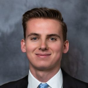 Stuart Smith joins ATREG after interning with the company for a year. In his role as Analyst, he is responsible for coordinating research and support activities around the disposition and acquisition of advanced semiconductor manufacturing facilities. This includes assisting with the development of marketing materials and coordinating outreach for new facilities that ATREG is bringing to market. Additionally, Stuart focuses on the analysis of the global semiconductor market and the identification of new opportunities related to operational manufacturing facilities.
Stuart graduated from the University of Washington in Seattle, Wash., USA with a double BS degree in Materials Engineering and Economics. While at university, he served as Undergraduate Research Assistant in an organic electronics lab, as well as Vice President of the Club Soccer Team. He also volunteered as a student mentor as part of the University of Washington Dream Project, assisting low-income high school students in the college application process and mentoring students in high school coursework, so they can meet graduation requirements.
VIEWPOINT 2020
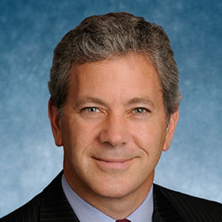
By Stephen Rothrock, Founder, President & CEO, ATREG, Inc.
Originally published in Semiconductor Packaging News on January 15, 2020
What does the future hold for Asian back-end manufacturing facilities?
 Until now, Asia has been the undisputed cradle for semiconductor back-end manufacturing fabs. More than 80% of OSAT facilities are currently located in the region, 50% of which in either China or Taiwan with the rest in a handful of countries including Thailand, Japan, Vietnam, Indonesia, or Malaysia.
Annual revenue among the top 25 OSATs amounted to $27.9 billion in 2018 and 65% of the A&T market is controlled by three Asia-based companies – Amkor, ASE, and JCET. The top eight OSATs (33%) account for $21.2 billion or 76% of revenue. Companies outside of the top 8 risk being an acquisition target if they cannot grow revenues beyond current levels.
But this picture could look very different in 2020. Chinese fabs are not producing significant wafers as the country is struggling to complete all of its fab builds (eight to 10 facilities out of 30 are not yet built). Advanced technology companies with back-end facilities in China are getting increasingly concerned because of the ongoing trade war between Beijing and Washington involving the introduction of 25 percent tariffs on phones, laptops, and tablets, IP protection, higher local labor costs, and the risk of overly centralizing production in just one location.
Each country is coming to the realization that they should keep their fabs closer to home. Here are a few concrete examples:
- Texas Instruments spending $2.5 billion to expand its existing 300mm fab in Richardson, TX
- Infineon investing €1.6 billion in a new 300mm wafer factory in Villach, Austria
- Bosch deciding to keep their investments in Dresden, Germany to build a brand-new 300mm fab
- STMicroelectronics announcing an expansion of existing sites in Europe
- Apple and Google moving some hardware production out of China
Only time will tell how the future of back-end manufacturing is going to unfold. The ATREG team will be keeping a finger on the pulse of those trends throughout 2020 to best inform advanced technology companies in their global back-end fab location choices.
For questions or comments on this article, please feel free to email Stephen directly.


