


ATREG ASSISTS ONSEMI WITH SALE OF TWO FABS IN THE U.S. AND EUROPE
ATREG is pleased to announce that it has successfully advised long-standing client onsemi on the disposition of two of its operational facilities in the U.S. and in Europe as part of the deployment of the semiconductor manufacturer’s fab-liter strategy. As onsemi transitions production to more efficient fabs within its network, the company will improve its cost structure by eliminating fixed costs associated with the sold fabs and lowering its unit costs.
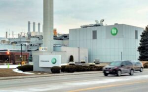 onsemi signed a definitive sale agreement with Diodes Incorporated for its operational 200mm fab located in South Portland, Maine in the U.S. The transaction is expected to close in the second quarter of 2022. The South Portland facility offers Diodes additional 200mm wafer fab capacity for analog products to accelerate its growth initiatives in the automotive and industrial end-markets.
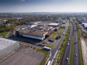 Earlier on February 8, 2022, onsemi also closed the sale of its automotive-certified 150mm facility based in Oudenaarde, Belgium with Belgian semiconductor company BelGaN Group BV, a consortium of investors and executives with extensive expertise in semiconductors. BelGaN plans to become a leading six- and eight-inch gallium nitride (GaN) foundry in Belgium.
“ATREG has been a strong advisor for onsemi and over the years has been involved in many fab transactions on behalf of the company,” explains Wei-Chung Wang, Executive Vice President of Global Manufacturing and Operations for onsemi. “For our South Portland facility, ATREG ran a highly competitive and expedited process. With regards to our Belgium fab, ATREG brought an innovative buyer that can take full advantage of available European funding to develop new technologies and prolong the fab’s life.”
“In an active market, one should not underestimate the time it takes to successfully complete a fab disposition. It is a testament to the onsemi team that these deals were executed in a relatively quick timeframe,” adds Stephen Rothrock, Founder, President, and CEO of ATREG. “We expect demand for 200mm brownfield fabs to continue to rise in 2022 as manufacturers attempt to mitigate the global chip shortage. With Europe’s IPCEI program, the 150mm Oudenaarde fab will not only continue chip production, but also update its manufacturing processes to new technologies over time.”
AVAILABLE FOR SALE: OPERATIONAL 150MM MEMS FAB, SOUTHWESTERN U.S.
 ATREG has been retained to facilitate the confidential disposition of an operational 150mm (200mm-capable) medical device-certified fab located in the southwest of the United States. The facility acts as a MEMS foundry focused on process module development, integration, industrialization, and manufacturing applied to sensors in the field of bio-MEMS and industrial applications. The opportunity includes a high-end, fully integrated line of approximately 60 150mm (200mm-capable) tools and a highly skilled team of approximately 20 employees averaging 15+ years of industry experience.
Opportunity highlights
- Building – 25,000 ft2
- Cleanroom – 10,000-ft2 Class 100 bay and chase with potential to increase to 12,000 ft2 and support space
- Capacity – 60,000 wafers per year; existing utilization space available for immediate production start
- Tools – Approx. 60 (with capabilities including, but not limited to, photolithography, wafer bonding, test, metallization, and metrology)
- Equipment process technologies – Fab currently operating at 150mm with some tools capable of 200mm; thin film and metal deposition, bonding and laminating
- Products – Implantable pressure sensors, biometric sensors, lab-on-chips, chemical and infrared sensors; various bonding and wafer dicing capabilities, disposition of laminates on various substrates, and microneedle; complex MEMS, bio-MEMS, and microfluidic devices
- Workforce – Highly experienced team of approx. 20 employees with an average of 15+ years of industry experience
- Certifications / ratings –ISO 9001:2015 and ISO 13485:2016 (medical device)
For more information or questions on this MEMS facility, please email our Vice President Annie Rothrock.
EXECUTIVE Q&A: JOHN VERWEY, ADVISOR, PNNL
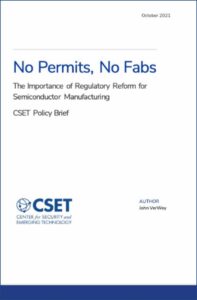 ATREG recently sat down with John VerWey, East Asia National Security Advisor at Pacific Northwest National Laboratory (PNNL) headquartered in Richland, WA, to discuss the findings of his latest report entitled No Permits, No Fabs – The Importance of Regulatory Reform for Semiconductor Manufacturing, a CSET (Center for Security and Emerging Technology) policy brief published in October 2021.
The ongoing global chip shortage, coupled with China’s heavy investments in indigenizing semiconductor manufacturing capabilities, has brought attention to the importance of semiconductors to the U.S. economy, the fragility of semiconductor supply chains, and the decline of U.S. chip making capacity over the past three decades. In part as a result of this attention, U.S. Congress has advanced legislation to appropriate $52 billion in funding for the CHIPS for America Act. Approximately $39 billion will likely go toward incentivizing semiconductor manufacturers to build new chip making capacity in the U.S. But more can be done to improve the resiliency of U.S. access to microelectronics beyond manufacturing incentives. The report outlines infrastructure investments and regulatory reforms that could make the United States a more attractive place to build new chip-making capacity and ensure continued U.S. access to key inputs for semiconductor manufacturing.
How did this report come about, John?
Georgetown University’s Center for Security and Emerging Technology (CSET) and PNNL established a relationship in 2021 that allows me to write papers for CSET on microelectronics-related subjects. CSET does best-in-class open-source research on emerging technologies in general, and the semiconductor industry specifically. For example, they have published extensive analysis on semiconductor supply chains and re-shoring semiconductor manufacturing. This report that I wrote for CSET, No Permits, No Fabs, is part of a series of CSET papers looking at policies and strategies for re-shoring semiconductor supply chains. There is also a forthcoming CSET report related to re-shoring advanced packaging.
In your opinion, what is the top reason why the U.S. is not able to build semiconductor fabs faster?
I think the top reason why the U.S. is not able to build fabs faster is the same reason the U.S. builds highways and railway infrastructure more slowly than peer countries – myriad (well-intentioned) regulations at the federal, state, and local level make it complicated to secure timely approval of large-scale construction projects. These regulations frequently require permits be issued in order for construction to proceed. And these permits in turn require application review periods, public comment periods, and appeals. This paper attempted to quantify the cumulative effect of these regulations on fab construction timelines.
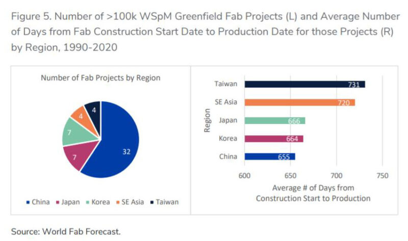
What factors do you think make Taiwan so successful at building fabs on time and on budget?
Our research has found that the Taiwanese government does a lot to ease the regulatory burden on semiconductor firms engaged in fab construction. This assistance takes many different forms – it will help prospective fab builders identify and acquire suitable plots of land, coordinate basic infrastructure investments (electricity, water, sidewalks), and even go so far as to set up job fairs to help these firms recruit local talent. Taiwan also has a series of free trade zones near their science parks – where most fabs are located, designed to facilitate efficient trading, warehousing, transport, and customs clearance processes that are critical to semiconductor manufacturers.
What role do environmental concerns play in U.S. greenfield fab construction? Can anything be done there to improve building timelines?
Environmental considerations are an extremely important determinant of fab construction timelines. Fabs require large plots of seismically inactive land with a reliable, affordable, and stable supply of water, electricity, transportation infrastructure, and nearby land for co-locating with suppliers essential for constructing and operating a modern fab. All these requirements implicate environmental considerations, from the Clean Air Act and the Clean Water Act to the National Environmental Policy Act (NEPA) and Toxic Substances Control Act. Federal regulators such as the Environmental Protection Agency (EPA) oversee some of these environmental regulations as well as counterparts at the state and local level. If regulatory reviews of fab construction environmental impacts are not adequately coordinated, it can slow construction timelines.
In the medium to long term, what would be the best answer? Increasing domestic production or stockpiling by coordinating with allies who already have existing production?
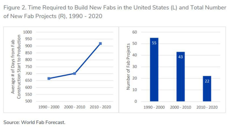
In the medium to long term, increasing domestic semiconductor fabrication capacity is optimal. But semiconductor fabs are not built overnight. So, increasing this capacity domestically will take time. And in fact, our research found that U.S. fab construction is much slower than the rest of the world. From 1990 to 2020, the time required to build a new fab in the United States increased by 38%, rising from an average of 665 days (1.8 years) during the 1990 to 2000 time period to 918 days (2.5 years) during the 2010-2020 time period. At the same time, the total number of new fab projects in the U.S. was halved, decreasing from 55 greenfield fab projects in the 1990-2000 time period to 22 greenfield fab projects between 2010 and 2020. As a result, coordinating with allies will also be very important.
How long do you forecast the global chip shortage to last?
It depends how you define the chip shortage. I think the chip shortage for DRAM and NAND chips will resolve sooner than the shortage of MCUs and substrate materials, for example. In general, lead times appear to be high but stable for most parts of the semiconductor supply chain. However, some of the most challenging parts of the supply chain shortage to resolve include substrate materials and semiconductor manufacturing equipment. On the former point, substrate manufacturers are making investments to increase capacity, but these investments will take time and some critical projects will not reach volume production until late 2022 or early 2023. On the latter point, semiconductor manufacturing equipment makers have recently reported that their ability to produce equipment is being adversely affected by lead times for semiconductors themselves. This could result in a damaging cycle whereby equipment makers cannot get the semiconductors they need to make their tools (etch, metrology, lithography, etc.), resulting in fabs not being able to increase their capacity to produce semiconductors, prolonging shortages overall.
In conclusion, what would be your best recommendation to expedite U.S. fab construction?
 In 2020, the White House Council on Environmental Quality compiled data on timelines for 1,276 Environmental Impact Statements (EIS) filed between 2010 and 2018 and found that National Environmental Policy Act (NEPA) reviews averaged 4.5 years. NEPA reviews are triggered when federal funds are directed towards large construction projects. Importantly, projects that receive CHIPS Act-affiliated funds may require NEPA reviews. This permitting process does not include the average of 1.86 years it takes to physically construct a semiconductor fab. In addition, an earlier report from the White House also identified pre-construction permits and operating permits required under the Clean Air Act as “the primary barrier to responsible and timely facility permitting” finding that “for some large projects, [this] permitting process can take 12 to 18 months.” I think careful analysis of how NEPA reviews and Clean Air Act reviews are conducted and coordinated across federal, state, and local regulators could help expedite fab construction timelines in the U.S.
What are the key agencies with greatest authority over this process?
Fab construction, like most infrastructure projects, implicates a wide variety of federal, state, and local agencies. The challenge is that no one agency has the greatest authority of this process. For example, our research found that when Samsung was expanding its foundry in Austin, TX in 2014, it had to secure approvals from the Environmental Protection Agency, the Department of the Interior, the U.S. Army Corps of Engineers’ Fort Worth, TX District, the State of Texas Commission on Environmental Quality, and the City of Austin’s Development Permitting office. This is an incomplete, but indicative list. In addition to the aforementioned agencies, the CHIPS Act, which is currently pending before Congress, tasks the Commerce Department with administering many of its incentive-related provisions.
About John VerWey
 John VerWey serves as East Asia National Security Advisor at Pacific Northwest National Laboratory (PNNL). In this role, he uses his background in strategic trade controls and U.S.-China technology competition to support U.S. government export control, supply chain security, and non-proliferation missions. He also serves as a consultant to Georgetown University’s Center for Security and Emerging Technology (CSET). Before joining PNNL, John worked for the U.S. Trade Representative where he was a staff liaison to the Committee on Foreign Investment in the United States (CFIUS), the U.S. International Trade Commission, and the Bureau of Industry and Security at the U.S. Department of Commerce. His research on the microelectronics industry has been published by the Journal of International Commerce and Economics, IEEE-Computer, and CSET, among others. John holds a graduate degree in international political economy from the London School of Economics as well as undergraduate degrees in Asian studies and history from Gonzaga University.
ATREG TO PRESENT AT GSA’S SILICON LEADERSHIP SUMMIT
![]() ATREG Founder, President & CEO Stephen Rothrock has been invited to speak at GSA’s Silicon Leadership Summit that will be held in person on May 12th at the Santa Clara Convention Center in CA. Stephen will be presenting “Covid, Chip Boom, And Supply Shortage: The New Normal For Global Semiconductor Manufacturing”.
ATREG Founder, President & CEO Stephen Rothrock has been invited to speak at GSA’s Silicon Leadership Summit that will be held in person on May 12th at the Santa Clara Convention Center in CA. Stephen will be presenting “Covid, Chip Boom, And Supply Shortage: The New Normal For Global Semiconductor Manufacturing”.
We look forward to connecting with you at the event and invite you to email us to set up an appointment to discuss your company’s global fab and cleanroom disposition or acquisition needs.
Click here for more information on the event.
In case you missed it, catch up with our Founder, President & CEO Stephen Rothrock’s Viewpoint 2022 contributed column published in Semiconductor Packaging News on January 27th.
 Global fab demand to continue to rise in 2022
To mitigate the global chip shortage, semiconductor manufacturers have left no stone unturned to increase capacity. Existing fabs are running at over 100% and tools are constrained. Many 200mm users are buying 300mm fabs to calibrate them back to 90nm, .13, and .18 nodes.
Within five years, the fab buyers’ market we knew suddenly morphed into a sellers’ market. As a result, a larger than usual number of fabs announced or closed worldwide in 2021 — nine total, marking a new turning point for global fab demand.
When it comes to back-end, only 6% of transactions took place in North America over the last 10 years, representing 32% of all transactions vs. 68% for front-end. Three back-end transactions happened in 2021 — InnoLight purchased Allegro MicroSystems’ Thai cleanroom, VIS acquired AUO’s Hsinchu, Taiwan fab, and SkyWater Technology Foundry bought the former 200mm BRIDG cleanroom in Osceola, FL.
Taiwanese OSATs are expected to sustain tight capacity supply for packaging services, chip probing, and final test operations through 2022, largely from international IC designers and automotive chip IDMs, with products boosting demand such as automotive CMOS image sensors, automotive MCUs, wireless communication chips, SiC and GaN power chips, and RF modules. Chinese OSATs also saw full capacity utilizations and order visibility through the end of 2021.
We can expect global fab demand to continue to increase and have another unprecedented year in 2022. Many challenges still lie ahead for our industry that must be resolved to overcome the global chip shortage sooner rather than later:
- Supply chain constraints must be addressed, still too many outages and fabs are lacking qualified talent
- Customer / supplier relationships are critical; we must address our geo-political environment to succeed
- An overarching pan-American manufacturing strategy is needed to ensure the U.S. retains its leadership
- We must find balance between Street’s push for financial performance and holding onto our fabs
- New sources of capital are essential to migrate more foundry capability over to the next generation
- We need to learn how to build new fabs faster if we are to build capacity and diminish our dependency on Asia
- Government incentives should be accessible to everyone, including smaller specialty product manufacturers
CONNECT WITH US AT GLOBAL INDUSTRY EVENTS
 Members of the ATREG team are excited to resume global travel this year to attend several global industry events on both sides of the pond in Q1 and Q2. Need to dispose of or acquire a brownfield fab or cleanroom? Looking for a brand-new greenfield building location or extra loading capacity? Don’t hesitate to email us to set up an appointment with one of our transaction experts at the event of your choice below to discuss your infrastructure-rich manufacturing asset needs for the coming months.
- Industry Strategy Symposium (ISS), April 3, Half Moon Bay, USA
- Women in Semiconductors, May 2, Saratoga Springs, USA
- GSA Silicon Leadership Summit, May 12, Santa Clara, USA
- JP Morgan Global Tech, Media & Communications Conference, May 23-25, Boston, USA
- Industry Strategy Symposium (ISS) Europe, May 30, Brussels, Belgium
- GSA European Executive Forum, June 2, Munich, Germany
- SEMICON China, June 15-17, Shanghai, China
We look forward to seeing you there!