
EXECUTIVE Q&A: SCOTT JONES, PRINCIPAL, KPMG & NEWLY APPOINTED ATREG ADVISORY BOARD MEMBER
 ATREG is pleased to welcome Scott Jones from KPMG LLP to its Advisory Board. As a Partner in KPMG’s Strategy Group based at the company’s Santa Clara, CA office, Scott leads the firm’s Semiconductor Practice for Advisory and focuses on M&A and operational improvement for semiconductor and other high-tech companies. During his 20-year career, Scott has led work on M&A transactions, operational transformations, R&D portfolio management, and turnaround and restructuring efforts across the semiconductor value chain. We recently sat down with Scott to discuss the impact of the COVID-19 pandemic on the global semiconductor industry.
How has COVID-19 impacted the semiconductor industry and what do you see as the long-term impacts of the pandemic?
While the short-term impact on the semiconductor sector is clearly negative, the long-term effects are likely an acceleration of the mega-trends that have been driving the industry over the past few years. The deployment of IoT devices, the use of AI, the rollout of 5G, and the adoption of autonomous vehicles will all be boosted by the resulting changes from the COVID-19 pandemic. In the near term, the adoption of these trends may be impacted by the economic downturn. But the push for greater remote working capabilities, upgraded communications infrastructure, the use of AI to solve complex problems such as mapping the RNA of new corona viruses and developing vaccines, as well as autonomous vehicles to support commute patterns will drive increased semiconductor demand in the long run.
 Do you expect the impact from the COVID-19 pandemic to lead to bankruptcies like we saw in the Great Recession of 2008?
We’ve already seen bankruptcies hit numerous sectors, but there have been fewer than in the 2008 Great Recession as the demand disruption has been more constrained to certain industries and bankruptcies have hit small businesses more than large companies. The exception would be companies that were extremely leveraged with high debt and also were in an industry that was impacted by a sudden loss of revenue, such as the entertainment and events industries.
How bad will the economy get and how long will an economic downturn last?
The economy will likely bottom in late Q2 or early Q3 and will then begin the process of recovery. Semiconductor recoveries generally take between two to three years for revenues to return to peak levels. Given the large levels of growth experienced in 2017 and 2018 followed by the correction in 2019, the return to peak revenue levels may not occur until 2022 or 2023. We expect the semiconductor industry to see significant drops in revenue in Q2 and Q3 of this year and then get back to seasonal revenue patterns and ship at normal levels by Q4 2020.
 What sectors of the semiconductor industry are most likely to benefit from the disruption caused by COVID-19?
Companies with exposure to the data center, PC, and communications infrastructure end-markets have seen a boost as the COVID-19 crisis has driven near-term demand for investments in these areas. The automotive segment has been hit the hardest as vehicle production has plummeted due to factory closures. The mobile handset segment has been lagging in performance due to market saturation for several years and has taken a big hit due to COVID-19 with the initial weakness in China followed by the downturn in Western markets. This segment will likely benefit from the 5G rollout and looking for that to be a catalyst to drive demand. The consumer segment is expected to weaken as it tracks mainly with world GDP growth, which is expected to dip this year due to COVID-19. Industrial, aerospace, and defense will likely have a temporary slow-down, but will return to normal demand levels rather quickly.
We have seen a lot of consolidation in the semiconductor industry in the last decade. Will this trend continue or will COVID-19 mute M&A activity?
We will not likely see that level of M&A again in the sector until more large semiconductor companies emerge from the increasing number of start-ups or the semiconductor companies that are growing inside platform technology companies such as Apple, Google, Amazon, and Microsoft. Until a new set of large companies emerge and tensions with China ease, we will struggle to get regulatory approval for large semiconductor deals. We do expect a large number of small acquisitions and carve-outs as companies optimize their portfolios and boost their IP and R&D capabilities.
 Are your clients pulling back on capital expenditures during this period of uncertainty or is there an assumption that markets will return to normalcy by Q3 / Q4? Are semiconductor companies preserving cash to mitigate a potential market downturn?
Our clients are moving ahead with capital investments for the most part. A recent survey we completed with GSA board members showed that only about 20% of the respondents are reducing their capital investments for the year. Companies entered the downturn with healthy balance sheets and the knowledge that companies need to invest through the downturn to emerge stronger and capture market share.
What advice would you give semiconductor industry executives about the global market outlook for the next six to 12 months?
Investing through the downturn is critical, but knowing where to invest is the hard part. Determining how demand patterns will shift due to the crisis and adjusting product roadmaps to align with that new demand profile is important as R&D dollars become more scarce in a downturn market. This is even more complicated when you have to align the investments of all of the partners in the ecosystem to get new products to market. Having visibility across your internal roadmaps and your partner ecosystem is important to ensure that your new product introductions generate the return-on-investment that you require.
About Scott Jones
 As a Partner in KPMG’s Strategy Group based at the company’s Santa Clara, CA office, Scott leads the firm’s Semiconductor Practice for Advisory and focuses on M&A and operational improvement for semiconductor and other high-tech companies. He began his career in finance at Intel and later became a program manager in the company’s Enterprise Product Group. After Intel, he covered the semiconductor sector at J.P. Morgan for the #1-ranked equity research team on Wall Street. Later, he joined AlixPartners to lead their Semiconductor Practice and the Digital Transformation Practice for the technology, media, and telecom sector.
During his 20-year career, Scott has led work on M&A transactions, operational transformations, R&D portfolio management, and turnaround and restructuring efforts across the semiconductor value chain.
Scott is a recognized thought-leader in the semiconductor industry who has authored a series of publications on R&D efficiency, portfolio management, as well as cost modeling and operations. He has moderated numerous panels and presented at industry and client events on advanced technology topics such as 3D/2.5D TSV, EUV, 3D NAND, and AI. He recently authored “Automotive Semiconductors: The New Ice Age” which highlights the $200 billion opportunity for semiconductors in the automotive end-markets.
Scott holds a Juris Doctorate from Santa Clara University, an MBA from the University of Arkansas, and a B.S. degree in Economics from the Centenary College of Louisiana.
AVAILABLE FOR SALE: ON SEMICONDUCTOR FAB, BELGIUM
Interested in a 200mm-convertible, 150mm manufacturing foothold in Europe? ON Semiconductor (Nasdaq: ON) has hired ATREG to find a buyer for its operational, automotive-qualified manufacturing facility located in Oudenaarde, Belgium, one hour’s drive from Brussels. Click here for a short fab video tour.
The company is looking for strategic partners willing to enter into a mutually beneficial arrangement that will facilitate an orderly transition of products from the Oudenaarde fab to other ON Semiconductor facilities. The opportunity includes a high-end, fully integrated line of 200mm-convertible, 150mm tools capable of manufacturing 19,000 wafers per month down to 0.35 μm.
Flanders Investment & Trade offers a series of tax incentives and government grants for international companies wishing to set up business in the region. More details are available in the Flanders Incentives Guide and the European Union R&D tax incentives.
![]() OFFERING HIGHLIGHTS
OFFERING HIGHLIGHTS
- Location – Close proximity to the world’s leading innovation and manufacturing hub in a stable region with a strong semiconductor ecosystem and extensive automotive presence
- Cleanroom – 4,300 m2 / 46,284 ft2 of cleanroom space located on a 10-acre campus
- Supply agreement – Potential for immediate, sustained cash flow with multi-year supply agreement with ON Semiconductor
- Tools –250 front-end manufacturing tools, approx. 80% of which are convertible to 200mm
- Products –35 μm to 2 µm low-, medium-, and high-voltage analog CMOS and BCD technologies
- Workforce – Team of 400 highly motivated and skilled employees with extensive experience managing a diverse array of technologies, including an experienced management team, 200 operators, 95 technicians, and 50 engineers
For more details on this offering, please email ATREG Business Associate Annie Rothrock.
ATREG CEO TO SPEAK AT MEPTEC WEBINAR
 ATREG is pleased to announce that Founder, President & CEO Stephen Rothrock will present U.S.-China Trade War: The Tariff Effects on the Global OSAT Market at MEPTEC‘s Semiconductor Industry Speaker Series Webinar on July 1st.
Stephen will provide insights into the current global tariff situation and how that has impacted IDMs and the OSAT market, drawing on some 20 years of international semiconductor manufacturing asset transactions.
Click here to sign up for the webinar.
In the meantime, don’t miss Steve’s contributed article on this topic on Page 14 of the spring issue of The MEPTEC Report.
AVAILABLE FOR SALE: ALLEGRO MICROSYSTEMS CLEANROOM, THAILAND
Allegro MicroSystems has retained ATREG to facilitate the sale of its production-ready, state-of-the-art cleanroom facility located in Saraburi Province, north of Bangkok, Thailand. Originally used for the assembly and testing of power IC products for the automotive industry, this manufacturing asset can accommodate the needs of multiple advanced technology sectors requiring a cleanroom environment.
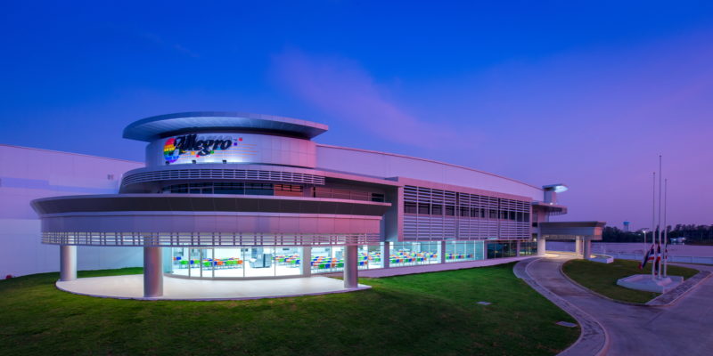
The 19.38-acre site consists of a 34,115 m2 (367,078 ft2) facility with cleanroom production areas, production support areas, office space, and unimproved shell space.
 As part of the campus, there is 30,692 m2 (7.58 acres) of developable land adjacent to the facility ready for future expansion that could effectively double the manufacturing capacity of the site.
This is an attractive acquisition opportunity for a global advanced technology manufacturing company looking for a cleanroom in the Asia-Pacific region at a price below replacement value.
To receive a comprehensive offering memorandum providing more details on this facility, please email ATREG’s Vice President Nick Papa.
GREENFIELD FAB OPPORTUNITY: MARCY NANOCENTER, NY
ATREG is assisting Mohawk Valley EDGE (MV EDGE) in promoting a semiconductor investment / expansion opportunity located near Utica in New York’s Mohawk Valley in partnership with Empire State Development Corporation (ESD). The fully permitted site, known as the Marcy Nanocenter, is one of the top development-ready sites in the world for semiconductor manufacturing. It offers up to one million ft2 of cleanroom space with either two 300mm fabs or three 200mm fabs.
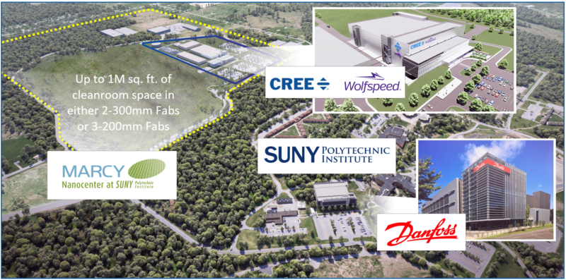
New York State (NYS), in collaboration with MV EDGE, National Grid, and Oneida County, invested $130 million for permitting, site development, road construction, and utility infrastructure to accommodate multiple semiconductor fabs. Additionally, NYS is offering globally competitive financial incentives for semiconductor companies that wish to establish additional manufacturing facilities at the site.
For two decades, NYS has provided cash, tax, and utility incentives totaling over $24 billion to its semiconductor ecosystem. It is committed to supporting further semiconductor investment to bolster its high-tech manufacturing ecosystem within its high-tech corridor. Of that, some $250 million has been allocated to support a seven-year $880 million semiconductor manufacturing research center at SUNY Polytechnic for Applied Materials. IBM has committed $2 billion over the next five years for R&D at the new AI Center and the Center for Semiconductor Research in Albany and Yorktown Heights, respectively.
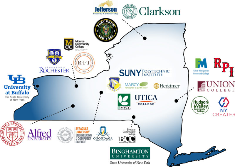
Known for its technology leadership and innovation, Upstate New York’s high-tech corridor has an established and growing semiconductor fab base, including facilities owned by GLOBALFOUNDRIES, Rohm, ON Semiconductor, and Cree | Wolfspeed. Equipment and consumables suppliers in the region support semiconductor and advanced electronics manufacturing, research, design, and packaging. They connect it to growth opportunities in market segments such as AI, IoT, high-performance computing, quantum computing, machine learning, blockchain, autonomous vehicles, AR / VR, medical devices, advanced energy, security, AgTech, and more. Additionally, many suppliers have expressed interest in co-locating at Marcy Nanocenter to increase efficiencies, create partnerships, and collaborate on R&D.
For more details on this greenfield offering opportunity, please email ATREG Business Associate Annie Rothrock.


