


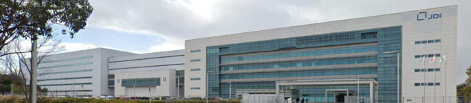
AVAILABLE FOR SALE: JDI OPERATIONAL FAB, HIGASHIURA, JAPAN
Japan Display, Inc. (JDI) has exclusively retained ATREG to assist with the disposition of its operational LCD G3.5 manufacturing facility located in Higashiura, Aichi Prefecture. Built out in 1998 (F-Tower and Energy Tower) and 2002 (C-Tower), the fab currently manufactures various display technologies (DSC, wearable, mobile, VR, and HUD) for multiple industries, including automotive. This facility could easily be converted to accommodate semiconductor manufacturing or other high-technology production, such as battery, solar, medical devices, or pharmaceutical. The site could also accommodate data center use.
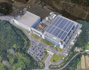 With easy access and proximity to Chubu International Airport, rail, and ports, this asset is a unique opportunity for a company that requires well-designed, infrastructure-rich advanced manufacturing space. JDI would also consider transferring tools to buyers interested in an operational sale.
OFFERING HIGHLIGHTS
- Total site area – 49.85 acres (201,774 m2)
- Total building area – 1,280,905 ft2 (119,000 m2) (three-building connected campus with five separate cleanrooms located in two buildings)
- Cleanrooms – Ballroom type offering 387,673 ft2 (36,016 m2) of manufacturing space
- Operating line specification – G3.5 glass substrate (600 × 720 mm) for small LCD panels (digital cameras / wearable devices)
- Certifications / ratings – IATF 16949 (automotive management system) and ISO 14001 (environmental management system)
For any questions or further details on this fab offering, please email ATREG’s Senior Associate Tom Johnson.
AVAILABLE FOR SALE: OPERATIONAL 150MM MEMS FAB, SOUTHWESTERN U.S.
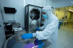 ATREG has been hired to help with the divestment of an operational 150mm (200mm-capable) medical device-certified fab based in the southwest of the United States. The facility acts as a MEMS foundry focused on process module development, integration, industrialization, and manufacturing applied to sensors in the field of bioMEMS and industrial applications. The opportunity includes a high-end, fully integrated line of approximately 60 150mm tools with capabilities including, but not limited to, photolithography, wafer bonding, test, metallization, and metrology.
Opportunity highlights
- Expansion potential – Leased 22,000-ft2 building and 6,000-ft2 cleanroom space (including approx. 500 ft2 of separate area for wafer dicing) can be extended up to 10,000 ft2 within the same building. Additional possible building expansion into parking lot of approx. 5,000 ft2
- Cleanroom – 6,000-ft2 Class 100 bay and chase with potential to increase up to 10,000 ft2 and support space
- Capacity – 60,000 wafers per year; existing utilization space available for immediate production start
- Equipment process technologies – Fab currently operating at 150mm with some tools capable of 200mm; thin film and metal deposition, bonding and laminating
- Products – Implantable pressure sensors, biometric sensors, lab-on-chips, chemical and infrared sensors; various bonding and wafer-dicing capabilities, disposition of laminates on various substrates, and microneedle; complex MEMS, bioMEMS, and microfluidic devices
- Workforce – Highly experienced team of approx. 20 employees averaging 15+ years of industry experience
- Certifications / ratings – ISO 9001:2015- and ISO 13485:2016-certified for quality management of medical devices manufacturing
For more information or questions on this MEMS facility, please email our Vice President Annie Rothrock.
SALE CLOSED: ONSEMI’S 200MM SOUTH PORTLAND, MAINE FAB
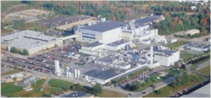 ATREG is pleased to announce that the acquisition of onsemi’s operational 200mm manufacturing fab located in South Portland, Maine, USA (SPFAB) by Diodes Incorporated officially closed on June 3rd, 2022. This fab divestment is part of onsemi’s fab-liter manufacturing strategy aimed at sustainable financial performance through gross margins expansion.
By integrating this U.S.-based facility into its existing wafer fabrication operations in Asia and Europe, Diodes will add 200mm capacity for analog products and be able to accelerate its growth initiatives in the automotive and industrial markets. Diodes plans to utilize the facility to qualify and manufacture CMOS and BiCMOS processes to support multiple analog product lines, including power management ICs, signal chain and standard products as well as several high-performance discrete product lines. As part of a multi-year wafer supply agreement, Diodes will also continue to manufacture onsemi’s products from SPFAB as onsemi completes the transferring of this production into its other wafer fabs.
“As we transition production to more efficient fabs within our global network, we will improve our cost structure by eliminating fixed costs associated with the sold fabs,” explains Wei-Chung Wang, Executive Vice President of Global Manufacturing and Operations for onsemi. “We are grateful to the ATREG team for helping us engineer this win-win transaction with Diodes.”
Click here to read ATREG’s press release. Click here to read Diodes’ press release.
WOLFSPEED INAUGURATES MOHAWK VALLEY SIC FAB
On April 25th after two years of construction, semiconductor powerhouse Wolfspeed officially inaugurated the world’s first, largest, and only 200mm silicon carbide (SiC) manufacturing facility at the Marcy Nanocenter near Utica, NY in the presence of federal and state officials, including New York State Governor Kathy Hochul. The $1 billion investment that will create over 600 new jobs within the first eight years of operation represents a significant step in bolstering the U.S. supply chain for advanced manufacturing and semiconductors. It will support growing electric vehicle, 4G and 5G mobile, as well as industrial markets. In addition to creating new jobs, Wolfspeed is actively working with education and business partners across the region to establish a robust pipeline for the next generation of high-quality, high-tech jobs in the Mohawk Valley, including those in advanced manufacturing.
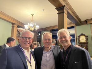 “It has been a pleasure bringing Wolfspeed to the Marcy Nanocenter and working hand-in-hand with Mohawk Valley EDGE and Empire State Development on this project for the past three years,” explains ATREG’s President and CEO Stephen Rothrock who attended the facility’s inauguration. “Congratulations to the Wolfspeed team for this amazing achievement!” (picture from left to right: Steven DiMeo, President & CEO, Mohawk Valley EDGE; Gregg Lowe, CEO, Wolfspeed; Stephen Rothrock, Founder, President & CEO, ATREG)
Click here to watch the Wolfspeed fab’s ribbon-cutting highlights. Click here to read New York State’s press release.
GSA 2022 SILICON LEADERSHIP SUMMIT RECAP
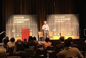 On May 12th, ATREG Founder, President & CEO Stephen M. Rothrock presented “Covid, Chip Boom, And Supply Shortage: The New Normal For Global Semiconductor Manufacturing” at GSA’s Silicon Leadership Summit held in Santa Clara, CA. Here is a summary of the presentation’s most important highlights.
The global chip shortage goes beyond a cyclical problem. The triggers to the crisis? Not only the Covid pandemic, but also semi’s fixation on maximizing gross margins and high profitability through high-capacity utilization and low inventory levels, as well as keeping fabs off the balance sheet. The security of the foundry model should be of concern to us all, along with the geopolitical risks existing not only around Russia and the Ukraine, but potentially with China and Taiwan.
Semi capacity shortage
So how do we solve the global fab shortage? Existing fabs are running at 100%+ capacity. Tools are constrained. Many 200mm users are buying 300mm and calibrating back to 90nm, .13 & .18 nodes. Semi manufacturing companies are considering restarting fabs. Fab construction companies are evaluating how they can renovate, re-engineer, and build faster. The question is: Can we build fabs fast enough in the U.S. like they do in Taiwan?
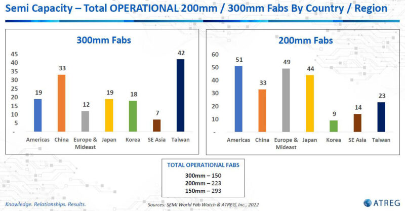
If we look at the world’s current operational fab count, what does that tell us?
- The large majority of all new fab projects between 2019 and 2020 were 300mm.
- The U.S. and Europe hold the most 200mm fabs, but Asia, Taiwan, and China have 50% more 300mm fabs than the U.S. and Europe put together (111 vs. 55).
- 300mm tools do exist – companies are making room for leading edge (Micron, SK Hynix, Samsung, Intel).
- The story of fab development is the story of the era of Western dominance leading to Eastern manufacturing dominance.
Increasing government incentives worldwide
Fab localization is now driven by politics rather than science or business. Local incentives will impact fab economics and influence future fab build locations. There is a need to recognize the interdependency of the global semi supply chain. Incentives are almost exclusively focused on leading-edge nodes, with 75% of planned CapEx committed to nodes more advanced than 15nm. Companies are projecting rapidly increasing demand for those areas, but those nodes are currently a small fraction of the market, particularly at 10nm and below. A significant portion of new fabs are coming online in China while only five new volume fabs will be starting production in the U.S. between 2021 and 2023, including Wolfspeed in NY, Intel in AZ and OR, and TI in TX.
This ratio improves in 2024/2025 – nine new fabs will spring out in the U.S. while only six are currently planned in China. There are very few eight-inch fabs out of these new ones as companies migrate to more advanced 300mm technologies. In fact, only one new volume eight-inch fab has started operating in 2022 (Wolfspeed NY) and none in 2023. If semiconductor manufacturers want to continue to pursue the expansion of 200mm production, available operational brownfield fabs become critical, with uses ranging from CMOS activities to more specialty operations such as GaN, silicon photonics, or MEMS. In the meantime, used 300mm equipment is becoming more popular, used for both 300mm production as well as adapted to 200mm manufacturing.
Dire labor shortage
Another major issue our industry is faced with is the lack of talent. How are we going to staff up all of these new fabs coming out of the ground, particularly in the U.S.? Talent was a major factor in Texas Instruments’ decision to acquire Micron’s 300mm fab in Lehi, UT last year. With this purchase, TI knowingly acquired the fab’s 1,215 employees, a wise strategic move for the company. As a result of the labor shortage, brownfield fab demand is at an all-time high, especially 200mm fabs and tools, driven by fear of allocation and the desire for internal manufacturing control. We expect the operational brownfield fab shortage to continue through to at least mid-2025. Mid-tier fabs that also have a critical place in the supply chain suffer from this shortage, particularly for newer technologies (compound semi, MEMS, sensors, silicon photonics, etc.) where convertibility to 200mm is extending lifecycles and increasing demand for 150mm fabs.
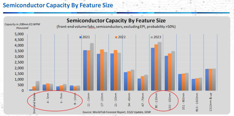
Semi capacity by feature size
The chart below shows that 90 to 350nm capacity (lagging-edge) makes up for about 27% of the market in 2022, compared to 10nm and below which makes up approx. 7% of the market today. It is important to keep in mind where the majority of capacity is located today despite all the global focus on sub-10nm and leading-edge investments. Lagging-edge nodes are still expected to grow by about 6% year-on-year over the next couple of years, primarily driven by internal fab expansions rather than greenfield fabs.
So what should we expect from the global manufacturing asset market going into 2022 and beyond?
- Semiconductors are foundational and supply chain constraints must be addressed – We must recognize the global interdependence of our global semi ecosystem. There are still too many outages (water, power, transportation) and the shortage of qualified workforce is growing worldwide.
- We must continue to focus on lagging-edge nodes – 200mm manufacturing serves markets that are not in the spotlight like other markets served by advanced 300mm manufacturing. Let’s keep in mind that there are very few new 200mm fabs being built. Seventy-five percent of planned CapEx are being done on nodes smaller than 15nm.
- It is critical to find balance between financial performance and holding onto our fabs – Between Wall Street’s push for financial performance and low gross margins, there is a pressing need to establish more hold on our domestic manufacturing assets.
- U.S. / European government incentives – The U.S. and Europe’s incentives of $40 to 50 billion for a 10-year investment program are not significant enough compared to China’s announced $130 to $140 billion. The U.S. has to do better than that if it wants to retain its semiconductor leadership in the world.
Click here to read our GSA presentation review on SemiWiki.
 The ATREG team looks forward to connecting with you in person at SEMICON West from July 11th to 14th at the Moscone Center in San Francisco, CA. During the conference, ATREG will be participating in the Fab Owners Alliance (FOA) Speed Dating event the afternoon of July 14th.
Please email us to set up an appointment with one of our advisors to discuss your manufacturing asset needs – whether you wish to sell / purchase an operational infrastructure-rich brownfield fab / cleanroom, you are looking for a greenfield fab location, or need extra loading capacity.
We can also meet up at these other upcoming Q3 events:
- SEMI MEMS & Imaging Sensors Summit, September 6-7, Grenoble, France
- GSA WLI WISH Conference, September 13, Santa Clara, USA
- GSA U.S. Executive Forum, September 27, Menlo Park, USA
We hope to see you there!