


ATREG ASSISTS MOHAWK VALLEY EDGE WITH SECURING CREE GREENFIELD SIC 200MM FAB IN UPSTATE NEW YORK
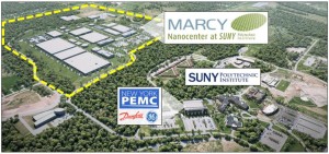
![]() The ATREG team is pleased to announce that as marketing agent for Mohawk Valley EDGE, an economic development organization in Oneida County, New York, it has assisted its client with securing Cree, Inc. as a new manufacturer to join New York state’s leading-edge semiconductor ecosystem. The major public-private partnership between the State of New York and Cree will contribute $1.2 billion over six years to build a state-of-the-art 200mm silicon carbide (SiC) wafer fabrication plant, invest $30 million on research and development, and employ at least 614 full-time employees at the Marcy Nanocenter on the SUNY Poly campus near Utica, New York. Upon completion of the fab in 2022, the new facility is expected to cover approximately 500,000 square feet, including 100,000 to 135,000 square feet of cleanroom space.
The ATREG team is pleased to announce that as marketing agent for Mohawk Valley EDGE, an economic development organization in Oneida County, New York, it has assisted its client with securing Cree, Inc. as a new manufacturer to join New York state’s leading-edge semiconductor ecosystem. The major public-private partnership between the State of New York and Cree will contribute $1.2 billion over six years to build a state-of-the-art 200mm silicon carbide (SiC) wafer fabrication plant, invest $30 million on research and development, and employ at least 614 full-time employees at the Marcy Nanocenter on the SUNY Poly campus near Utica, New York. Upon completion of the fab in 2022, the new facility is expected to cover approximately 500,000 square feet, including 100,000 to 135,000 square feet of cleanroom space.
“The remit of our client Mohawk Valley EDGE was clear – bring world-class technology players to the Marcy Nanocenter greenfield site to help address the growing demand from automotive, communications infrastructure, and industrial markets,” explains Stephen Rothrock, President and CEO of ATREG. “Cree is a U.S. semiconductor powerhouse specializing in one of the most promising technologies with applications in two of today’s highest-growth sectors – electric vehicles and 5G. ATREG is honored to contribute to reinforcing New York state’s position as a leading U.S. innovation hub in power electronics and radio frequency (RF). We look forward to bringing more high-caliber technology players to the upstate New York campus in coming months.”
 “The ATREG team has been instrumental in helping us secure this new addition to Mohawk Valley’s growing technology industry,” adds Steve DiMeo, President of Mohawk Valley EDGE. “Today’s manufacturers are always looking for better, smarter ways to produce vital electronics components. Cree’s high-voltage power electronic devices are more compact, efficient, and cheaper to produce. ATREG’s deep knowledge and understanding of the global semiconductor supply chain combined with their long-standing relationships with the world’s executive technology leaders helped us identify and facilitate the right match. It’s a win-win for all!”
New York State will provide $500 million in performance-based, capital grants from Empire State Development to reimburse a portion of Cree’s costs of fitting out the new facility and acquiring and installing machinery and equipment, as well as $1 million in Excelsior Jobs tax credits.
There is still space available on the Marcy Nanocenter site near Utica. Should your company be interested in exploring a greenfield fab building opportunity in upstate NY, please email our CEO Stephen Rothrock at stephen.rothrock@atreg.com.
Click here to read the Governor of New York state’s press release.
Click here to read the Cree press release.
ATREG SPEAKS AT IMAPS’ 2019 SYMPOSIUM IN BOSTON
Want to know where to locate your next back-end manufacturing facility? Come hear ATREG President & CEO Stephen Rothrock at 10:15 am on October 3rd at IMAPS’ 52nd IMAPS International Symposium on Microelectronics (International Microelectronics Assembly & Packaging Society) in Boston, USA to find out!
In a presentation entitled Semiconductor Manufacturing Strategy: Where In The World To Locate A Fab Or Cleanroom?, Stephen will provide insights into how to best approach manufacturing strategy decisions in the context of today’s global semiconductor landscape.
![]() The global market for advanced technology manufacturing assets is becoming ever tighter, compelling semiconductor companies, including OSATs (outsourced semiconductor assembly and test), IDMs (integrated device manufacturers), and foundries, to carefully explore all available options when planning manufacturing operations relating to fabs, tools, and cleanrooms. Despite the semiconductor industry’s optimistic growth forecasts, global uncertainty generated by the continuing trade wars between the U.S. and China is causing anxiety among advanced technology companies and forcing them to constantly rethink their manufacturing strategies – buy vs. build, best fab location, risk mitigation, local incentives, etc. In 2018, semiconductor companies showed increased renewed interest in U.S.-based manufacturing in the midst of a continued lack of 200mm and 300mm capacity. As we have seen with the recent sale of Texas Instrument’s 150mm / 200mm facility in Greenock, UK to Diodes Incorporated and Vanguard International Semiconductor Corporation’s acquisition of GLOBALFOUNDRIES’ 200mm Fab E3 in Tampines, Singapore, 200mm fabs are still in very high demand and manufacturers are becoming increasingly proactive as they look to expand capacity.
The global market for advanced technology manufacturing assets is becoming ever tighter, compelling semiconductor companies, including OSATs (outsourced semiconductor assembly and test), IDMs (integrated device manufacturers), and foundries, to carefully explore all available options when planning manufacturing operations relating to fabs, tools, and cleanrooms. Despite the semiconductor industry’s optimistic growth forecasts, global uncertainty generated by the continuing trade wars between the U.S. and China is causing anxiety among advanced technology companies and forcing them to constantly rethink their manufacturing strategies – buy vs. build, best fab location, risk mitigation, local incentives, etc. In 2018, semiconductor companies showed increased renewed interest in U.S.-based manufacturing in the midst of a continued lack of 200mm and 300mm capacity. As we have seen with the recent sale of Texas Instrument’s 150mm / 200mm facility in Greenock, UK to Diodes Incorporated and Vanguard International Semiconductor Corporation’s acquisition of GLOBALFOUNDRIES’ 200mm Fab E3 in Tampines, Singapore, 200mm fabs are still in very high demand and manufacturers are becoming increasingly proactive as they look to expand capacity.
 In 2019, infrastructure-rich cleanroom manufacturing assets are going to continue to play an essential part in shaping these strategies to ensure global competitive advantage as more wafers are needed and more facilities are being built worldwide, particularly in China. Despite a slowdown in semiconductor mergers and acquisitions activity, the global semiconductor market will continue to consolidate as the manufacturing needs of advanced technology companies evolve with market changes. This has put a strain on manufacturing space and resulted in a number of new capital projects and expansions that may become difficult to fulfill in the current market. A shortage of existing manufacturing space means cleanrooms and operational fabs will sell at a premium. Many companies are also looking at greenfield sites with local government incentives playing an active role. Running in tandem, there is still a shortage of used and new production tools with lead times in excess of one year to purchase new fabs from OEMs (original equipment manufacturers) or equip new fabs.
Drawing on some 20 years of infrastructure-rich manufacturing asset dispositions and acquisitions as well as a series of real-world fab transaction case studies, ATREG Founder, President and CEO Stephen M. Rothrock will provide insights into how to best approach manufacturing strategy decisions in the context of today’s global semiconductor landscape.
CONNECT WITH US AT Q4 GLOBAL EVENTS
 Need to discuss the divestment or acquisition of an infrastructure-rich manufacturing asset or looking for a brand-new greenfield opportunity, extra loading capacity, or used fab tools? Please email us to set up an appointment with a member of our team at any of these upcoming global industry events:
- IMAPS’ International Symposium on Microelectronics, October 1-3, Boston, USA
- ITPC, November 3-6, Maui, USA
- SEMICON Europa, November 12-15, Munich, Germany
- SIA Awards Dinner, November 7, San Jose, USA
- GSA Awards Dinner, December 5, Santa Clara, USA
- SEMICON Japan, December 11-13, Tokyo, Japan
We look forward to seeing you there!