


GUEST COLUMN: COVID-19 DRIVES RISE FOR SEMICONDUCTORS
From gloom to boom for some industry segments
By Christian Dieseldorff, Senior Principal Analyst for Semiconductors, Industry Research & Statistics Group, SEMI
The semiconductor industry should feel lucky not to be the restaurant or travel business. How is it possible that the COVID-19 pandemic turns from gloom to boom for some industry segments?
Historically revenue and investments (such as fab equipment spending, shown in figure 1 below) ride the same roller coaster. Typically, one or two years of positive growth are followed by one or two years with negative change rates. The reasons behind this cycle follow predictable patterns – build-up of overcapacity, increase in inventory, and falling chip prices. It’s rare to see three or more consecutive years of growth, as we saw for fab equipment spending from 2016 to 2018.
Sometimes this cycle is amplified by outside forces such as major macroeconomic disruptions. Macroeconomic trends do not always correlate very well to the semiconductor industry cycle – except when things are really bad. The worst down years for the industry were in 2001 when the tech bubble burst, and 2008-2009 with the real estate bust.
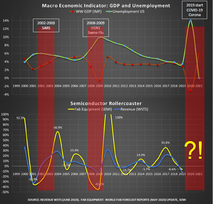
Figure 1: Roller coaster of the semiconductor industry and macroeconomic impact
So what’s happening now? According to IMF (April 2020), worldwide GDP has dropped from 2.9% in 2019 to -3% in 2020, worse than during the 2008-2009 financial crisis which was -0.6% worldwide (-2.6% for the U.S.) This year’s Great Lockdown is now the worst recession since the Great Depression in the mid-1930s (-13% for the U.S. in 1932).
U.S. unemployment reached about 14% in May 2020. As of mid-June, over 45 million people have filed for unemployment. That is the highest rate since the Great Depression in the U.S. (1931-1940). The last time unemployment hit the 10% marker was in 2009.
Coincidentally, the last two major pandemics have overlaid the last two major economic crises and the accompanying dips in the semiconductor industry: SARS in 2002-2003, and H1N1 in 2008-2009.
In 2012, MERS had less impact on the Western hemisphere, but interestingly, fab equipment spending and revenue still dropped. While the prior pandemics were not the root cause of the past economic crises, COVID-19 is the first pandemic to cause an economic crisis, affecting the economy and the semiconductor industry on a large scale. These macroeconomic indicators – GDP and unemployment – suggest a bad year for the industry, as seen in 2001 and 2008-2009.
How challenging it is to forecast is reflected in the revenue forecast by some of the leading market research firms. Forecasts made before the beginning of 2020 painted a rosy picture for the industry, as shown in figure 2 below.
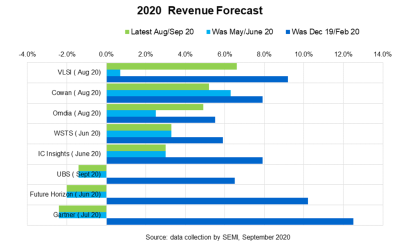
Figure 2: Revenue forecasts by leading market research firms
The average revenue forecast was about 7% when the year 2020 started (dark blue bar), with all leading analysts predicting industry growth. As the events of the virus unfolded, projections were revised and the average dropped to about 1% in May / June (light blue bar), with many analysts actually predicting negative change rates for the year. Further revisions revealed that some analysts see the industry bouncing back with an average 2% growth projected as of August. The range of predictions is still wide, from about -2% to +6%.
What changed in the first half of 2020?
Two main factors have moved revenue forecasts. The pandemic has increased the need for technology. Meanwhile, in the face of uncertainty caused by COVID-19 and U.S.-China trade tensions, companies began to stockpile. Of these two factors, the stockpiling may be the most unpredictable one.
Although demand for new cars and smartphones has declined in the first half of the year, stay-at-home orders caused a surge for communication technology (such as IT and personal devices), in addition to surges in gaming and healthcare electronics.
Surprisingly, stockpiling behavior also drove sales and investment in 2Q20, driving up demand for cloud service, memory (enterprise SSDs), and notebooks and tablets. Some companies, mainly memory makers, reported record sales in 1Q20, and demand exceeded supply in some cases.
In addition, the pandemic has caused delays or complete stops of construction projects and production ramps. Supply chain issues were reported, travel restrictions prevented the delivery of equipment, and engineers could not travel to sites to install equipment.
For the second half of 2020, it’s expected that some of these limitations will be lifted or eased. Businesses re-opening and pent-up demand ensure a strong second half of 2020.
As a result, SEMI’s latest World Fab Forecast for fab equipment spending in 2020 changed from 3% growth (predicted as of February 2020) to 8% growth, as illustrated in figure 3 below.
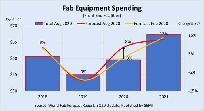
Figure 3: Fab equipment spending over time
Regions with the highest fab equipment spending in 2020 are China, Taiwan, and Korea, with US$ 14 to 15 billion each. Next are Japan and the Americas, spending US$6 to 7 billion each. Europe and Mideast has about US$ 3 billion and South East Asia is below US$ 2 billion.
Of all chip sectors, memory will see the largest spending increase in 2020, growing US$3.7 billion, or 16% year-over-year (YoY). 3D NAND spending will log the largest percentage surge this year, expanding 39%. Foundry, the next largest sector in equipment spending for 2020, is forecast to rise US$2.5 billion, or 12% YoY, to US$23.2 billion.
Fab equipment spending by product type reflects the trends in end-user demand, as per figure 4 below.
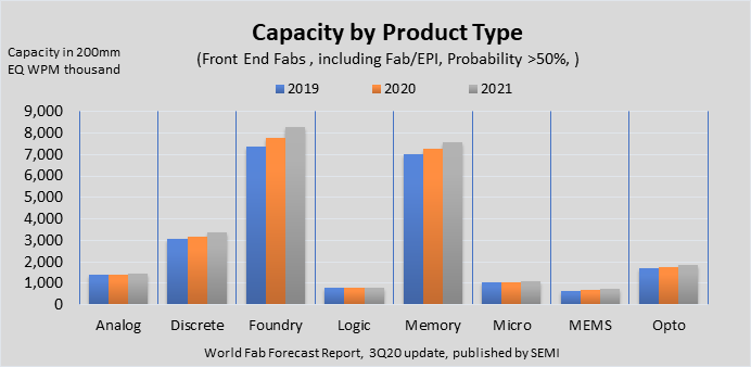
Figure 4: Installed capacity by product type
The foundry sector has the largest installed capacity in 2020 and 2021. Growth rate in 2020 is 6% and another 6% is expected in 2021. Closely following is memory with steady growth rate of about 4% in 2020 and another 4% in 2021. Slower growth for DRAM is expected to be only 3% in 2020 and a more vigorous 5% in 2021 while 3D NAND jumps 17% in 2020 and another 13% in 2021.
Although smaller in total value, other product segments will also experience strong growth. Fab equipment for image sensors will rise 4% to US$3 billion in 2020 and jump 11% to US$3.4 billion in 2021. Analog spending will grow a robust 48% in 2020 and rise 6% in 2021, an expansion chiefly driven by equipment investments for mixed-signal / power fabs. MPU equipment spending, on the other hand, will decline -18% in 2020 and then rise by only 9% in 2021.
Some regions have evolved to be a stronghold for certain product segments. Taiwan solidly leads in foundry, Korea in memory, and China in foundry, memory, and discretes. SEMI’s latest World Fab Forecast still shows Taiwan with most installed capacity in 2020, but China will pull ahead in 2021, adding capacity in both memory and foundry. The same scenario will repeat in 2021, as Chinese-owned companies are responsible for more than 60% of all capacity added by the industry.
The uncertainty of COVID-19, followed by trade war tensions, continues into the second half of 2020. New realities include high unemployment, business closures, and debt defaults. As new waves of infection and responses emerge, with continued work and school from home, the need to communicate is stronger than ever. Demand grows for semiconductors for data center infrastructure and server storage, along with gaming and healthcare electronics.
All leading market research firms expect positive growth in 2021, projecting an average 12% in revenue growth. This mirrors expected positive macroeconomic indicators, such as worldwide GDP of 5.8%. Fab equipment spending is also expected to rise, growing 13% to a new record of over US$67 billion.
Technology is what the semiconductor industry does, and technology sends it to new heights, even as other industries struggle to survive.
The SEMI World Fab Forecast report covers more than 1,300 fabs and lines, including capacity and technology by fab and construction investments. The report shows 21 new construction projects – ranging from R&D to volume and including high- and low-probability parameters – starting in 2020. China accounts for the most (nine) of the new projects, followed by Taiwan at five, Southeast Asia and the Americas at two each, and Japan, Korea, and Europe / Mideast at one each. The report also tracks 18 new construction projects planned to begin next year – 10 in China, four in the Americas, three in Taiwan, and one in Europe / Mideast.
About Christian Dieseldorff

With over 30 years of experience in the semiconductor industry, Christian serves as Senior Principal Analyst for Semiconductors in SEMI’s Industry Research & Statistics Group in Milpitas, CA. For 15 years, Chris has been engaged in various engineering and management positions in start-up R&D and pilot lines at Siemens (Munich), IBM (New York), International Sematech (Austin, TX), and Infineon (San Jose, CA).
Since 2002, Chris has served as director of market research and analysis for the semiconductor industry first for Strategic Marketing Associates, and since 2007 for SEMI. Chris holds an engineering degree from the University of Applied Science in Isny, Germany.
SPOTLIGHT: EU SEMICONDUCTOR INCENTIVES IN BELGIUM
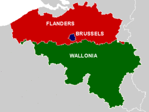
![]() If your company is looking to invest in a semiconductor manufacturing foothold in Europe, Flanders Investment & Trade (FIT) in Belgium offers a series of tax incentives and government grants for international companies wishing to set up business in the northern region of the country. Some additional incentives from the European Union may also be available to potential buyers interested in local fabs. “Belgium is highly committed to the semiconductor industry,” explains Wim Sohier, Science and Technology Counselor – Americas and Head of FIT in San Francisco, CA. “The Government of Flanders alone earmarks USD700 million annually to supporting innovative activities and spends almost 3% of its GDP on R&D.”
If your company is looking to invest in a semiconductor manufacturing foothold in Europe, Flanders Investment & Trade (FIT) in Belgium offers a series of tax incentives and government grants for international companies wishing to set up business in the northern region of the country. Some additional incentives from the European Union may also be available to potential buyers interested in local fabs. “Belgium is highly committed to the semiconductor industry,” explains Wim Sohier, Science and Technology Counselor – Americas and Head of FIT in San Francisco, CA. “The Government of Flanders alone earmarks USD700 million annually to supporting innovative activities and spends almost 3% of its GDP on R&D.”
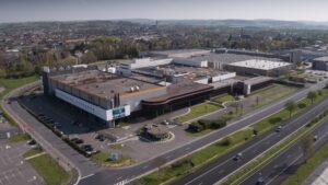 A great example illustrating that commitment is ON Semiconductor’s operational, automotive-qualified manufacturing facility. Located on a 10-acre campus in Oudenaarde, the fab offers a high-end, fully integrated line of 200mm-convertible 150mm tools capable of manufacturing approximately 4,400 wafers per week down to 0.35 μm, a 4,300 m2 Class 1 cleanroom space (additional floor space of 1,800 m2 allows for expansion of existing four-wall manufacturing capacity), and a workforce of approximately 400 highly skilled employees. There is potential for immediate, sustained cash flow with a multi-year supply agreement with ON Semiconductor for any buyer interested in the facility.
Despite nearly 71% of the 320 available front-end fab tools being 200mm-convertible, the conversion would carry a significant cost for the facility’s ultimate buyer. To remedy the issue, the Flanders Government have indicated that they would provide a capital match of up to 50 to 60% of the cost associated with the purchase of new tools and tool upgrades. Financial support for projects could go up to 60% of the projected cost in case of research and 50% of the projected cost in case of development. The specifics of the prospect’s plan, technology, new tools versus upgrade, the totality of the project, its employment, plans for the campus, the international reputation of the prospect, all play into an optimal outcome with maximized commitment from Flanders.
 Another incentive to consider is pure location-related – being in close proximity to one of the world’s leading innovation and manufacturing hub in a stable region with a strong semiconductor ecosystem and extensive automotive presence. This includes imec, the renowned Belgian R&D hub for nano- and digital technologies, whose state-of-the-art sites and cleanrooms yield the opportunity to complement any buyer’s in-house innovation capacity, opening up huge potential to tap into the even more ambitious funding from the EU government for collaborative R&D.
In addition to these already very generous incentives, the Flanders Government offers other cash grants, as follows:
- Federal fiscal incentives for R&D (e.g. not paying social contribution on salary, revenue from patents being 85% tax exempt, or a five-year tax ruling with frozen corporate tax rates)
- European project funding under the Horizon Europe framework (project-based research together with a university, imec or another European company)
You will find more details on Flanders and European tax incentives and grants in the documents below:
For more details on the ON Semiconductor Oudenaarde fab, please email Annie Rothrock, ATREG’s Director of Business Operations or click here for a short video tour of the fab.
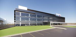
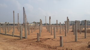
IT’S ALL HAPPENING AT THE MARCY NANOCENTER, NY
It’s been busy the past few months at the Marcy Nanocenter in Upstate New York! The foundation of Cree | Wolfspeed’s state-of-the-art greenfield 200mm-capable SiC fab is set and vertical work has begun! Construction of the $1 billion factory near the SUNY Polytechnic Institute Utica campus started earlier this year and has continued despite the current coronavirus pandemic.
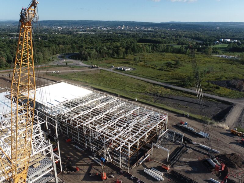
The building is expected to be finished in 2021 and the factory scheduled to start production of its first silicon carbide wafers in early 2022. Hiring for the facility is well under way. The construction plans include:
- A 454,000-sq. ft. fabrication building with 112,000 sq. ft. of cleanroom space
- A connected four-floor administration building
- A separate 100,000- sq. ft. central utility building will be connected via a bridge
You can find more detailed information on Cree | Wolfspeed’s new Mohawk Valley fab web site.
 Should you be looking for a U.S.-based greenfield fab opportunity, the Marcy Nanocenter still has a million sq. ft. of cleanroom space available adjacent to the Cree | Wolfspeed fab for additional fab construction. ATREG is assisting Mohawk Valley EDGE (MV EDGE) in promoting New York’s Mohawk Valley in partnership with Empire State Development Corporation (ESD). The fully permitted site is one of the top development-ready sites in the world for semiconductor manufacturing. New York State (NYS), in collaboration with MV EDGE, National Grid, and Oneida County, has already invested over $130 million for permitting, site development, road construction, and utility infrastructure to accommodate multiple semiconductor fabs. Additionally, NYS is offering globally competitive financial incentives for semiconductor companies that wish to establish additional manufacturing facilities at the site.
Please email Annie Rothrock, ATREG’s Director of Business Operations, should you be interested in learning more about this opportunity.
AVAILABLE FOR SALE: ALLEGRO MICROSYSTEMS CLEANROOM, THAILAND
 The result of state-of-the-art engineering and construction, the Allegro MicroSystems facility located in Saraburi Province, north of Bangkok, Thailand was completed in 2015.
The fab was carefully sited outside of, and at an elevation 8m higher than the 2011 Thailand flood line. Construction included a sophisticated soil compaction technique, along with a piling foundation system, on top of which the pristine facility sits.
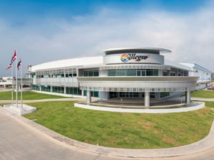 The existing production-ready ballroom cleanroom can be easily extended into an already established interior shell. The property also boasts plenty of space for future expansion and buildings. This manufacturing asset can accommodate the needs of multiple advanced technology sectors requiring a cleanroom environment.
This offering is an attractive opportunity for a global advanced technology manufacturing company looking for a cleanroom in the Asia-Pacific region.
For more details on this facility, please email Nick Papa, ATREG’s Vice President.