


EXECUTIVE Q&A: AJIT MANOCHA, PRESIDENT & CEO, SEMI
![]() ATREG recently sat down with Ajit Manocha, President and CEO of SEMI headquartered in Milpitas, CA, to discuss the United States Innovation and Competition Act (USICA) and its impact on the U.S. semiconductor industry.
ATREG recently sat down with Ajit Manocha, President and CEO of SEMI headquartered in Milpitas, CA, to discuss the United States Innovation and Competition Act (USICA) and its impact on the U.S. semiconductor industry.
Do you believe that the funding currently included in the USICA will be substantial enough to rejuvenate U.S. semiconductor manufacturing?
I do believe the $52 billion in emergency appropriations included in USICA would be a significant short-term catalyst for U.S. semiconductor manufacturing. The funding is front-loaded, but it only lasts for five years. For the longer term, the bipartisan FABS Act would create a permanent 25% tax credit for investments in facilities and equipment to produce semiconductors and semiconductor manufacturing tools. SEMI strongly supports this bill because it would create a permanent, transparent, and immediately “investable” incentive to make U.S. semiconductor and semiconductor equipment more globally competitive.
Is there significant support for this additional investment tax credit?
 The FABS Act tax credit was introduced by Senate Finance Committee Chairman Wyden and Ranking Member Crapo – the leaders on tax policy in the Senate – and has significant support from key Senators. With the current focus on the crucial importance of a secure and resilient supply of semiconductors around the globe, many countries are implementing incentives and tax credits as key tools to grow their role in the worldwide semiconductor ecosystem. The availability of robust incentives in other countries and the lack of federal U.S. incentives have been key factors driving the location of more overseas semiconductor manufacturing facilities. The investment tax credit in the FABS Act is a necessity for the U.S. to keep pace.
Will there be any limitations on foreign-owned entities receiving funding or will all U.S.-based manufacturing projects be eligible to receive funding?
There are no limitations specific to foreign-owned entities receiving funding in the authorizing statute. Foreign-owned fabs such as the one TSMC is building in Arizona will contribute to the resiliency and security of the U.S. semiconductor supply chain.
Will the majority of available funding be distributed through national grants? Will there be a reimbursement system based on company investment levels?
The Senate USICA bill devoted most of the USICA funding to the incentive / grant program – roughly $40 billion of the $50 billion appropriated. The specific mechanisms for reimbursement, and whether there will be general target percentage of investment, is not detailed in the statute. This would come from the Department of Commerce as they implement the program.
Will there be any limitations on the number of money allocated to one project? One company? One state?
 The only limitation in the statute is a “soft cap” of $3 billion per project which can be exceeded with a presidential certification. SEMI is working to ensure funding is available to upstream semiconductor equipment and materials companies to meet the goal of strengthening the entire semiconductor supply chain in the United States. In terms of geographical distribution, SEMI members operate semiconductor supply chain facilities in 25 states, so there are many possible locations that could see expansions.
Do you anticipate portions of the funding being allocated for smaller-scale projects within the semiconductor industry? E.g. for areas such as MEMS, back-end, etc.
Yes, it is critical that funding is available for smaller-scale projects as well. The chip shortage has clearly shown how any weak links among devices, equipment, and materials can lead to lines down for customers. It makes perfect sense for funding to be used wherever it is needed to fortify the overall supply chain.
About Ajit Manocha
 Ajit is President and CEO of SEMI. Throughout his career, he has been a champion of industry collaboration as a critical means of advancing technology for societal and economic prosperity.
Ajit was formerly CEO at GLOBALFOUNDRIES. Prior to this, he held the role of EVP of Worldwide Operations at Spansion and earlier served as EVP and Chief Manufacturing Officer at Philips / NXP Semiconductors. He began his career at AT&T Bell Laboratories as a research scientist where he was granted more than a dozen patents related to semiconductor manufacturing processes that served as the foundation for modern microelectronics manufacturing. He has served on the boards of SEMI, SIA, and GSA.
Ajit is active on global advocacy and workforce development issues and has served on the President’s committees for Advanced Manufacturing Partnerships and the President’s Council of Advisors on Science & Technology (PCAST).
In 2021, VLSIresearch added Ajit to its Semiconductor Industry Hall of Fame for his leadership of SEMI efforts to address geopolitical trade tensions as well as for his initiative in navigating the many challenges of the COVID-19 pandemic impacting SEMI and the microelectronics industry. In 2020, Ajit was inducted into the Silicon Valley Engineering Hall of Fame and VLSI named him an All Star of the Semiconductor Industry for his visionary leadership in 2019 to restructure SEMI to represent the expanded electronics supply chain.
ICYMI: SEPTEMBER 8 MEPTEC WEBINAR RECORDING
![]() Missed our President & CEO Stephen Rothrock‘s MEPTEC webinar on September 8th?
Missed our President & CEO Stephen Rothrock‘s MEPTEC webinar on September 8th?
Click here to view the full event recording now available on YouTube and catch up on all the details of Stephen’s global fab / OSAT manufacturing asset market overview and global government incentives for greenfield fab construction.
For any questions on the event content, please email us.
GLOBAL FAB EQUIPMENT SPENDING SOARS TOWARDS THE $100 BILLION MARK IN 2022. WHAT’S NEXT?
By Christian Dieseldorff, Senior Principal Analyst for Semiconductors, Industry Research & Statistics Group, SEMI
Powered by pandemic-generated spending, global semiconductor equipment investments for front-end fabs are expected to reach nearly US$100 billion by the end of 2022. This year, with surging demand for electronics, spending will top $90 billion. The World Fab Forecast published by SEMI in early September 2021 highlights these consecutive, record-setting years in Figure 1 below:
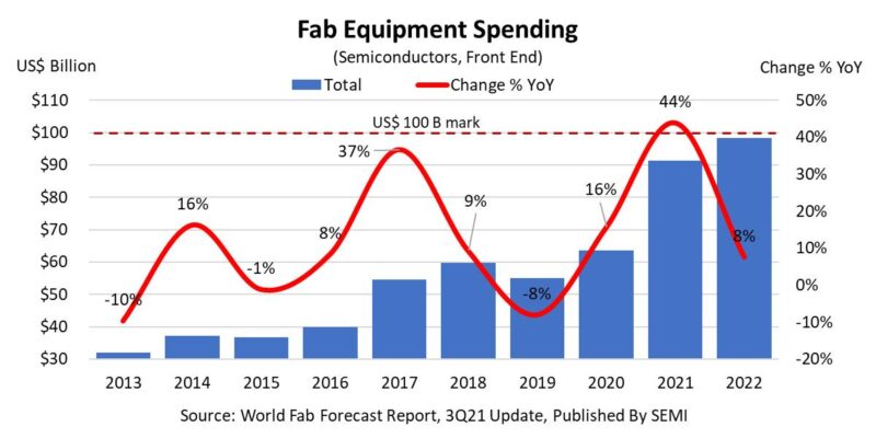
Figure 1 – Fab equipment spending for semiconductor front-end facilities from 2013 to 2022 (Sept. 1, 2021, SEMI)
These spending records will mark a rare three consecutive years of growth that began in 2020, bucking the historical cyclic trend of a one- or two-year expansion, followed by a year or two of tepid growth or declines. The last time the semiconductor industry saw more than two consecutive years was from 2016 to 2018 and before that in the mid-1990s.
What’s next?
If the industry follows its historical trend, a slowdown should arrive in 2023. SEMI’s 300mm Fab Outlook to 2024 which was updated on September 1st, 2021 does look further out, forecasting through 2024 for 300mm fabs, which represent the majority of investments for semiconductors worldwide. Indeed, SEMI’s data confirm this expectation for 2023 with about 0% growth (flat). After that one-year dip, however, the industry will likely see another dramatic increase for equipment spending in 2024, breaking 2022’s record to pass the US$110 billion mark.
The bulk of these huge investments in 2021 and 2022 will come from new semiconductor lines that started construction in the prior one to two years. Similarly, the bump in spending in 2024 will be mostly for new lines starting construction in 2021 and 2022. On average, a new line beginning construction mid-2022 will be ready for equipment move-in by the end of 2023. Factors such as cleanroom size, product type, or fab location can cause variation in this general timeline. Pending market conditions, high spending in 2024 may spill over into 2025 and beyond.
SEMI’s World Fab Forecast report provides rich details by quarter about new cleanroom lines starting construction in 2021 and 2022, for a total of 44 known new high-volume semiconductor lines (including all those, a probability of greater than 50%). The number is even higher if including lower probability, such as rumored projects or those with unsure financial backing. Figure 2 below shows in which regions these new lines will be built:
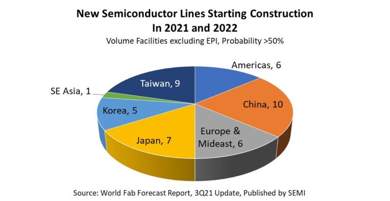
Figure 2 – New semiconductor front-end lines starting construction in 2021 and 2022 (Sept. 1, 2021, SEMI)
Of course, this quarterly report represents currently known semiconductor projects. It is likely that some companies will announce more new projects that will push spending even higher than SEMI’s September 2021 published forecast. Most of these new lines are for 300mm wafer size (35), with fewer fabs at 200mm or smaller wafer size. Down the road, these 44 projects will require combined equipment spending of US$195 billion, as shown in Figure 3 by region:
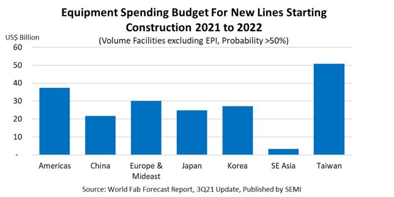
Figure 3 – Total equipment spending budget for new semiconductor front-end lines starting construction in 2021 and 2022 (Sept. 1, 2021, SEMI)
Turning away from these record-breaking spending levels to consider the effect on industry capacity, these 44 new lines will add about 1.9 million wafers per month (in 200mm equivalents), as illustrated in Figure 4 below:
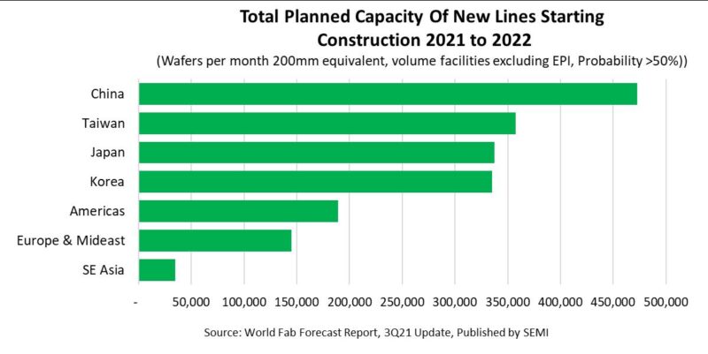
Figure 4 – Total planned capacity (in 200mm equivalents) of new semiconductor front-end lines starting construction in 2021 and 2022 (Sept. 1, 2021, SEMI)
The four regions with the largest capacity increases are China, Taiwan, Japan, and Korea. As shown in Figure 4, China leads the pack in capacity growth, with new projects planned to add 470,000 wafers per month (in 200mm equivalents). Over 95% of this capacity is contributed by Chinese-owned companies, a proportion that has changed dramatically. Back in 2017-2018, about half of all planned capacity for new line projects came from international companies doing business in China.
While China plans to add the most capacity, far more than most regions, projected equipment spending is quite low (next to lowest of all regions). This is explained by reviewing where the capacity will be added. In China, most of the increase will be for mature technologies rather than leading-edge nodes. About half of China’s increased capacity will be added for foundries, with nodes in the 55 to 28nm range, 24% for discrete in the 500 to 350nm range, just 13% for memory, and 14% for MEMS and analog.
In second place for capacity growth will be Taiwan, with about 360,000 wafers per month (all in 200mm equivalents). Japan and Korea will be close behind at 335,000 wafers per month. Meanwhile, the Americas will add about 190,000 wafers per month and Europe and Mideast about 150,000 wafers per month.
Fab equipment spending is a solid indicator of industry strength. With the pandemic world running short on chips, the industry is doing very well. Just within the last 10 years, the industry has twice seen three-year spurts of consecutive growth in fab equipment spending. This unusual pattern leads total spending to jump over the $90 billion mark in 2021 and just miss the $100 billion mark in 2022. Meanwhile, SEMI’s analysts are already tracking 44 additional construction projects starting in 2021 and 2022 that are budgeted for another $195 billion, spread out over coming years through 2024. There is no sign of lower investment levels in the near future.
SEMI’s Word Fab Forecast report has served the industry for over 20 years, with detailed project and facility information about construction and equipment investment, capacity, product types, and technologies. The most recent update dating September 1st, 2021 lists 1,417 facilities and lines globally, including 129 facilities and lines starting volume production from 2021 to 2032 with various probabilities.
About Christian Dieseldorff
 With over 30 years of experience in the semiconductor industry, Christian serves as Senior Principal Analyst for Semiconductors in SEMI’s Industry Research & Statistics Group in Milpitas, CA. For 15 years, Chris has been engaged in various engineering and management positions in start-up R&D and pilot lines at Siemens (Munich), IBM (New York), International Sematech (Austin, TX), and Infineon (San Jose, CA).
Since 2002, Chris has served as director of market research and analysis for the semiconductor industry first for Strategic Marketing Associates, and since 2007 for SEMI. Chris holds an engineering degree from the University of Applied Science in Isny, Germany.