


GUEST COLUMN: THE KEY FACTORS IMPACTING SEMICONDUCTOR MARKET GROWTH
By Dr. Handel Jones, CEO, International Business Strategies
The global semiconductor market is projected to amount to $850 billion in 2027 compared to $467 billion in 2018, with the potential to reach $1 trillion in 2030. While the U.S. leads the pack in processor-based designs, Europe is ahead in power semiconductors, South Korea in memory, Taiwan in foundry, and Japan in image sensors. At the same time, China is transforming from a technology follower into a technology leader, particularly when it comes to 5G infrastructure and edge devices.
TSMC is in high-volume production at 7nm while Samsung is expected to be the technology leader at 4nm, with the adoption of EUV. TSMC is also projecting that 3nm will be in volume production in 2022. ASML has demonstrated excellent technology and business innovation in developing EUV scanners that will allow migration to 5nm and 2nm or potentially 1.5nm if gate-all-around (GAA) structures are successful.
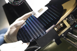
 3D NAND Flash is in initial production at 96 layers, with 128 layers in initial development. It is expected that with some modifications to the device structures, 256 layers and potentially 512 layers can be cost-effective and will be in volume production between 2022 and 2024. New non-volatile memory technology may, however, be needed to have a significant increase in memory density and lower gigabyte costs. DRAM products are being manufactured in 15nm, and while 13nm and 12nm are possible, there are indications of saturation. There will also be a need for new device structures to replace the capacitor-transistor structures of DRAM.
Legacy-silicon-based technologies are reaching their theoretical limits, and while new materials can provide some benefits, the expectation is that these benefits will be relatively small in many areas. An exception is the adoption of silicon carbide (SiC) for power MOSFETs to support electric vehicles. The market for SiC MOSFETs is estimated at $15.7 billion in 2027 compared to $490 million in 2018, and the key factor for this growth will be the effectiveness of the supply chain ecosystem in competing with SiC-based IGBT structures. Modules are another key requirement for high-power applications.
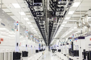
The slowing of manufacturing complexity will not impact the growth of the semiconductor market. The reality is that semiconductor market growth will accelerate as artificial intelligence (AI) and machine learning applications become mainstream. Without major enhancements to process technologies, more wafers will need to be manufactured and new wafer fab facilities will need to be built.
In many high-growth areas, there will be shortages of manufacturing capacity, which will include mature technology nodes. An example is that while there will be excess wafer fab capacity at 28nm in 2019 and 2020, there will be shortages in 2023 or 2024 because of strong demand for Internet of Things (IoT) and multimedia applications. The result is that the foundry market for 28nm is projected to be $15.2 billion in 2027 compared to $9.8 billion in 2018. There will also be the need to build large wafer fab capacity for 5nm and smaller, and a 5nm wafer fab will cost $15 billion for 40K to 50K WPM. Growth of SiC consumption will also be constrained by capacity for crystal pulling and epitaxial wafer supply. A similar supply shortage situation can also apply to raw silicon wafers for 5nm and smaller as well as to specialty wafers such as FD SOI if the appropriate investments are not made in additional capacity ahead of when market demand emerges.
 Specialty packaging is another area of high growth, including wafer-level fan-out technologies. There will also be ongoing challenges in getting the tight-tolerance substrates needed for the multi-chip modules for both small form factor applications such as smartphones and high-voltage and high-power applications such as on-board charging of electric vehicles. Consequently, it is important to have a long-term and positive perspective on the growth of the semiconductor market and to ensure that enough manufacturing capacity is built to meet the demand of high-growth applications.
The enhancements in the capabilities of the semiconductor supply chains have been excellent over the past few decades, and many companies, including materials vendors, equipment vendors, and wafer manufacturers, are involved. The enhancements over the next few decades will be even greater because of the adoption of blockchain and machine learning.
The semiconductor industry has to be regarded as an exciting growth industry rather than as a mature industry where innovation is low. While some areas have plateaued, the upward growth slopes of many segments are expected to accelerate. Semiconductor manufacturing is the foundation of the semiconductor industry, and the semiconductor industry is the foundation of the electronics industry. Therefore, it is important to be involved in the full supply chain for semiconductors and to embrace the adoption of emerging AI-based blockchain and machine learning technologies. The impact of AI and machine learning over the next 10 to 15 years will be far greater than anything previously experienced in the semiconductor industry.
About the author
 Dr. Handel Jones founded International Business Strategies, Inc. (IBS) based in Los Gatos, Calif. in 1988 to provide global technology industry leaders with strategic consulting. Prior to IBS, Dr. Jones managed 1500+ engineers at Rockwell International, which included avionics, communications, and semiconductors. He participated in the French government’s advanced technology initiatives and was involved in several due diligence projects on a number of IPOs. A China expert, Dr. Jones has published several books, including China’s Globalization (How China Becomes No. 1), Chinamerica (McGraw Hill), and Artificial Intelligence: How AI and IA Reshape the Future. He has contributed to a variety of publications, including The Wall Street Journal, The Economist, The New York Times, Forbes’ blog, China Daily, Global Times, EE Times, and Xinhua to name just a few.
SEASON’S GREETINGS!
 As 2018 comes to an end, the ATREG team wishes you a very festive holiday season! On behalf of our valued clients, we will be making donations to the following local and international non-profit organizations:
- L’Arche International, an international federation dedicated to the creation and growth of homes, programs, and support networks for people with and without intellectual disabilities to live mutual relationships, share daily life, and build a community together
- The Homelessness Project / The Society of St. Vincent de Paul, who, for the past 180 years, has been leading individuals to join together to offer person-to-person service to the poor and the suffering
- Global Partnerships, an international impact investor with the mission to expand opportunity for people living in poverty via micro-financing
Wishing you and yours health, happiness, and success in 2019!
SEE YOU AT ISS 2019 IN HALF MOON BAY
 Members of the ATREG team will attend SEMI’s Annual Industry Strategy Symposium (ISS) from January 6 to 9 in Half Moon Bay, Calif. Please email us to set up an appointment with one of our experts to discuss your specific infrastructure-rich manufacturing asset needs, including cleanrooms, fabs, and secondary tools.
We also look forward to connecting with you at these other Q1 global industry events:
- Morgan Stanley TMT Conference, February 25-28, San Francisco, USA
- SEMICON China, March 20-22, Shanghai, China
- ISS Europe, March 31-April 2, Milan, Italy