
CREE / MARCY NANOCENTER UPDATE
Since announcing the selection of the Marcy Nanocenter site near Utica, NY for the construction of its new 200mm SiC fab last September, Cree has hit the ground running with construction planning, industry partnerships, and local community involvement. The semiconductor powerhouse is due to occupy the uppermost tier of the greenfield site which offers room for future expansion. Cree has chosen Albany-based construction company Exyte to build the new Marcy facility.
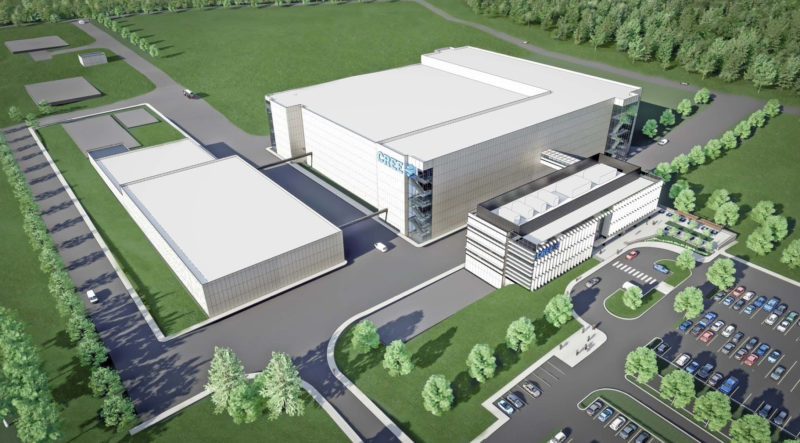
Fab construction schedule
- Q4 2019: Begin work in Albany
- 2020: Start of fab construction
- Q2 2021: Fab expected to be built and ready for equipment
- Q2 2022: Fab expected to ramp up for production
- 2024: Fab fully operational
 The project will utilize 55+/- AC on the site. As the market for silicon carbide grows, Cree expects to fit out the fab to full capacity, representing a total investment of $1.23 billion. New York state will provide $501 million in performance-based incentives on a reimbursement basis. Mohawk Valley EDGE, along with OCIDA, Oneida County, and Community Foundation, will provide local incentives and benefits via a PILOT agreement. Cree will operate at SUNY Poly in Albany until the Marcy fab is completed, then relocate employees and tools from Albany and their Durham fab to the NY site.
Cree’s NY fab by the numbers
- Direct jobs created: 614+ within eight years
- Fab site size: 480,000 sq. ft. on 55 acres
- Investment: $1.23 billion
- New York incentives: $501 million
Recently announced partnerships
- The expansion of an existing multi-year, long-term silicon carbide wafer supply agreement to more than $500 million with STMicroelectronics
- A silicon carbide partnership with ABB to deliver automotive and industrial solutions
- A strategic partnership with ZF to advance the electric powertrain with a SiC-based inverter
Talent recruitment
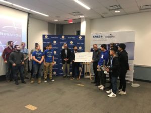 On November 18th, Cree staff starting their recruitment and university outreach to the Albany community, including a career fair at SUNY Poly to recruit talent for the upcoming new fab. It also gifted the university $25,000 to support STEM programs and help train SUNY students to work at the new facility after graduation, including internships and research opportunities.
Cree and New York Center for Research, Economic Advancement, Technology, Engineering, and Science (NY CREATES) also successfully completed the first SiC test wafers at the SUNY Poly Albany campus, just days after the Sept. announcement. Dedicated staff from both Cree and NY CREATES worked together on the tests, marking the start of collaborative efforts in Albany. This test is key to ensuring the qualification of the fab for ongoing production when it ramps in 2022.
Local community involvement
 On December 12th, Cree employees and representatives volunteered for the Rescue Mission of Utica by organizing donations, wrapping gifts, and preparing dinner baskets for over 200 families in need this Christmas across Utica and the Mohawk Valley.
For more information
Two additional tiers next to Cree’s on the Marcy Nanocenter site still remain for additional greenfield fab opportunities. Please contact Annie Rothrock at ATREG should your company be interested in learning more.
EXECUTIVE Q&A WITH DEB GARAND, ACCENTURE STRATEGY
![]() ATREG recently sat down with Deb Garand, Semiconductor Managing Director at Accenture Strategy based in Boston, Mass., to discuss the continuing consolidation of the global semiconductor industry. Semiconductors are the core driver of any innovation supporting a wide range of industries and connected devices. Accenture offers deep domain expertise across the industry, including practical and operational experience, as well as deep relationships and experience across the value chain.
ATREG recently sat down with Deb Garand, Semiconductor Managing Director at Accenture Strategy based in Boston, Mass., to discuss the continuing consolidation of the global semiconductor industry. Semiconductors are the core driver of any innovation supporting a wide range of industries and connected devices. Accenture offers deep domain expertise across the industry, including practical and operational experience, as well as deep relationships and experience across the value chain.
One of Accenture’s key focus areas is to help the industry grow and compete as the global landscape changes and adapts to consolidation and digitalization. This represents an opportunity for semiconductor companies to look more broadly across their businesses, including opportunities to monetize new products and services. Accenture brings new capabilities to help companies be more relevant in their marketplace, while ensuring that their operations are as future-facing and innovative as their technology.
 What are your key takeaways from the continuing consolidation that has been happening in the global semiconductor industry over the past three years?
Clearly, there has been a growing trend towards specialization, driven by the emergence of exciting new applications such as high-performance computing, artificial intelligence, machine learning, autonomous driving, communications, and virtual reality, among others. As a result, we have seen non-semiconductor players who were typically end-customers or systems integrators acquiring semiconductor device capabilities. In essence, they are entering the semiconductor industry to gain access to the specialization they need. Examples include Microsoft and Google who now have internal design teams developing data center chips.
At the same time, pure-play semiconductor companies are expanding their horizontal and vertical capabilities across the value chain. While this is not consolidation-focused, it is an important trend to recognize as it enables companies to leverage M&A activities to achieve expansion across the value chain. It also significantly changes the dynamics of data sharing because unlikely partners who did not previously share sensitive and secure IP and data in the past are now having to get creative with data sharing. This means that semiconductor companies are starting to look at new ways to share sensitive data which could have an overall benefit for the broader industry.
Do you anticipate this consolidation to continue for much longer? Is there any end in sight?
To answer this question, it is important to consider the primary reasons for consolidation. Clearly, consolidation is not affecting R&D expenditures or the rate of innovation, so cost synergies are not a driving reason. Rather, the key drivers are generally low interest rates and high liquidity in the West, and government policy and incentives for the semiconductor industry in China. If history repeats itself, the current consolidation wave should slow down when the liquidity reduces.
 A secondary reason for consolidation is specialization, market focus, and segment leadership. Companies that divest or invest in order to get more specialized generally have the best returns and are rewarded by the market with higher valuations. A tertiary reason for M&A activity is non-semiconductor players acquiring semiconductor capabilities initially enabled by leading-edge foundry services. This has enabled companies such as Apple, Siemens, Tesla, Google, and Amazon to have better control of their respective supply chains and end-products. Finally, advancement in semiconductor devices beyond the linear line-width shrinks have provided new applications and market growth.
How is this consolidation beneficial for semiconductor customers?
Customers are continually looking for more so-called integrated solutions from their vendors and consolidation enables semiconductor companies to achieve that. Semiconductor offerings have become extremely sophisticated and cost-intensive and it does not always make sense for one company to develop all the pieces of the puzzle. Advancements in application spaces that begin to overlap areas that were quite distinct provide a strategic driving force for growth through acquisitions.
Where do you see the industry moving toward and what impact will geopolitical issues have on the industry?
Even with the recent trend towards consolidation, we believe the number of semiconductor companies will continue to increase. One reason is that increased investment has spawned a large number of semiconductor start-ups. Another is that end-customers and OEMs are moving up and across the value chain to acquire semiconductor capabilities.
Current geopolitical issues have potential for longer-term impact on the semiconductor industry. Any disruption to the global semiconductor ecosystem could slowly grow for semiconductor companies. In addition, large supply chain uncertainties could potentially affect investment in both technology and scale.
About Deb Garand
 Deb serves as Managing Director in Accenture’s High-Tech and Semiconductor Strategy Practice. She has over 20 years of experience in competitiveness, growth strategy, business transformation, operating model design, MA&D, organizational alignment (including business and technology alignment), and strategic change management.
Deb has worked globally with semiconductor companies across the entire value chain, including those producing alternatives to traditional silicon. She is a U.S. patent holder (15718/499) for Cryptographic Data-Share Control for Blockchain in the semiconductor industry. Deb holds a BA from the University of New Hampshire and is a certified Balanced Scorecard Professional.
ATREG IN THE NEWS
 We are making headlines in the semiconductor press again!
In case you missed it, the guest editorial entitled Top 6 considerations when selecting a fab location authored by our President & CEO Stephen Rothrock was published in the November / December issue of Chip Scale Review. It discusses the factors that advanced technology manufacturers should take into account for a successful global fab site selection, including:
- Transaction and consolidation trends
- Financial investment
- Existing loading and supply agreements
- Local incentives
- Trade wars and tariffs
- IP protection
Click here to read the full article.
SEE YOU AT ISS IN HALF MOON BAY!
 Members of the ATREG team will attend SEMI’s Annual Industry Strategy Symposium (ISS) from January 12 to 15 in Half Moon Bay, Calif. Please email us to set up an appointment at the event with one of our experts to discuss your specific infrastructure-rich manufacturing asset needs for 2020, including fabs, cleanrooms, and secondary tools / equipment. We can also advise you on available global brownfield and greenfield fab options.
We also look forward to connecting with you at these other upcoming global industry events next year:
- Goldman Sachs Technology and Internet Conference, February 11-13, San Francisco, USA
- IMAPS International Conference on Device Packaging, March 3-5, Fountain Hills, USA
- SEMICON China, March 18-20, Shanghai, China
- ISS Europe, April 1-3, Brussels, Belgium


