
2022 is coming to a close. ATREG wishes you and yours a healthy and festive holiday season! Our team is very grateful and thankful for the continued loyalty and support of its valued clients and partners. This year again for the holidays, we will be making donations on their behalf to the following local and international non-profit organizations:
 World Health Organization – More than 7,000 people working to lead and coordinate the global effort to prevent, detect, and respond to global pandemics.
- The Homeless Project / The Society of St. Vincent De Paul – Leading individuals who join together to offer person-to-person service to the poor and the suffering for the past 180 years.
- L’Arche International – An international federation dedicated to the creation and growth of homes, programs, and support networks for people with and without intellectual disabilities to live mutual relationships, share daily life, and build a community together.
- Global Partnerships – An international impact investor with the mission to expand opportunity for people living in poverty via micro-financing.
Wishing you and yours health, happiness, and success in 2023!
The ATREG Team
SALE COMPLETE: ONSEMI POCATELLO, ID FAB
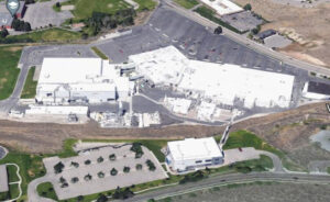 ATREG is pleased to announce that the sale of onsemi’s operational 200mm manufacturing fab located in Pocatello, Idaho, USA to LA Semiconductor has officially closed.
Located on a 33-acre campus with over 50,000 ft2 of cleanroom space and over 550,000 ft2 of building space, the onsemi’s ID fab currently produces 0.35 µm to 1.5 µm analog CMOS, BCD, advanced discrete, and custom technologies.
“In addition to our South Portland, Maine and our Oudenaarde, Belgium fabs, this is the third manufacturing asset disposition that ATREG has helped us with over the past 12 months,” explains Wei-Chung Wang, Executive Vice President, Global Manufacturing & Operations for onsemi. “This divestment is a continuation of onsemi’s fab-liter manufacturing strategy aimed at achieving a sustainable financial performance through upscaling capacity for products in our key automotive and industrial markets.”
Click here to read the full press release.
AVAILABLE FOR SALE: 200MM ELMOS FAB, DORTMUND, GERMANY
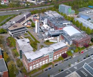 Elmos Semiconductor SE has retained ATREG to assist with the disposition of its operational 200mm, automotive-certified manufacturing facility located in Dortmund, Germany. This cost-effective facility produces low-, medium-, and high-voltage CMOS and MEMS for automotive, industrial, and consumer products. The opportunity includes a high-end, fully integrated line of 200mm tools capable of manufacturing down to 0.35μm.
OPPORTUNITY HIGHLIGHTS
- Automotive experience – 25+ years of automotive manufacturing experience; regular customer audits
- Capacity – Current loading of approx. 1,800 wafers / week based on an average of ~24-mask layer process; four-wall capacity of approx. 2,400 wafers / week
- Multi-year supply agreement – Elmos requires a 3+-year supply agreement which can provide the buyer with immediate and sustained cash flow as Elmos ramps down production
- Process capabilities – Facility currently manufacturing geometries down to 0.35μm (most equipment capable of handling 0.25μm geometries)
- Equipment process technologies – 130 well-maintained 200mm front-end tools
- Certifications – Automotive-certified, IATF 16949, ISO 14001, ISO 45001, and ISO 50001
- Process technologies – Low-, medium-, and high-voltage automotive CMOS processes, including deep-trench SOI and MEMS (CMOS-based) processes
- Cleanroom overview – Efficient 2 484 m2 / 26,738 ft2 ISO Class 4 cleanroom, including 593 m2 / 6,383 ft2 of expansion space within four walls; potential to expand outside of existing four walls
- Highly skilled labor – Approximately 230 highly experienced employees
- IP licensing opportunity – Opportunity to license relevant IP
For questions or more details about this offering, please email ATREG Vice President Annie Rothrock.
SEMICON EUROPA 2022 GLOBAL FAB MARKET RECAP
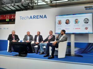 It was a pleasure to reconnect with the global semiconductor industry at SEMICON Europa in Munich, Germany last month. Our sincere thanks to everyone who attended ATREG’s global fab market overview presentation on November 17th, and in particular to Alexander Gorski from Infineon, Dr. Patrick Leinenbach from Bosch, Rudi De Winter from X-FAB, and Abdelkarim Moharram from Bechtel for participating in the subsequent panel discussion Greenfield vs. brownfield – how global government incentives could tip the fab balance. Here are a few highlights from this session.
Many different market growth drivers are constantly shaping our semiconductor manufacturing needs, including automotive electrification and digitalization, AI, super computing, wireless communications (5G, 6G, satellites, IOT), digital computing, and carbon neutrality. To meet all this demand for more chips, we need more fabs, so let’s look at the latest global fab breakdown by country / region to see where we’re at.
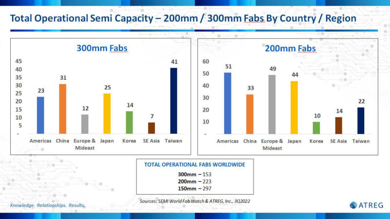
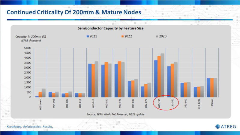
Existing brownfield fabs and mature nodes will remain critical for the future of our industry as we continue building on existing semiconductor ecosystems and clusters to keep manufacturing costs under control. Existing fabs are currently running at 100%+ capacity and tools are constrained. Many 200mm users are buying 300mm tools and calibrating them back to 90, 130, and 180nm nodes. As the recessionary market ahead of us continues to test the resilience of the global supply chain, we will likely see more innovative business models from chip makers such as fab sharing.
Compound semi, GaN, GaA, SiC, and MEMS users want fabs, but is greenfield the answer? Bosch, Wolfspeed, and several others think so. Most new fab projects between 2019 and 2020 were 300mm. The U.S. and Europe have the most 200mm fabs, but Taiwan and China have twice as many 300mm fabs. After a surge in fab transactions following the 2008-2010 recession, there has been a significant tapering off from 2015 to 2020 with an average of 4.5 fabs sold per year. It’s been a buyers’ market for the last five years, but that is rapidly changing in today’s global economic climate. Thirty-seven 200m fabs have changed hands over the past 10 years, and in 2021 that trend continued with five (of which four are 200mm). The 2021 comeback can be explained by several factors, including tight supply constraints, risks associated with the current geopolitical environment, companies put on allocation, as well as steady price increases.
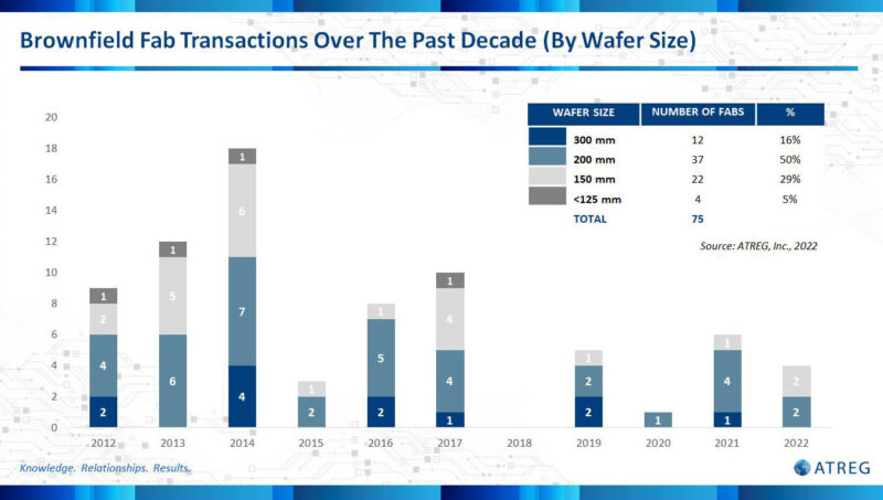
While core 200mm products / geometries (90 to 350nm) continue to make up a huge portion of today’s demand, the majority of greenfield fabs being built are at 300mm (except for specialty, e.g. SiC). Existing 200mm brownfield fabs remain critical to serve industries that don’t need leading-edge products (e.g. automotive). With greenfield expansions mainly focused on 300mm leading edge, chip makers will still have to convert some 200mm fab tools to 300mm to continue keeping up with demand.
The race for CHIPS Act funding for greenfield fabs in the U.S. is now well under way. We can expect a similar situation in Europe next year as EU countries recently reached common position on their Chips Act aimed at doubling the EU’s global semiconductor market share from 10% to at least 20% by 2030 to ensure the EU’s future technological sovereignty.
 In case you missed them, catch up with the latest trends in the global fab asset market with a couple of recently published articles.
ATREG’s President and CEO Stephen Rothrock and Yole Group’s President and CEO Jean-Christophe Eloy discussed the state of the global semiconductor fab market in a post-COVID world. Click here to read the full article entitled The 2023 global fab landscape: opportunities and obstacles published on November 10th.
ATREG also contributed its 2023 Executive Viewpoint Fab Sharing: A Smart Move For Chip Makers published in the November / December issue of Semiconductor Digest. Click here to read the full article on pages 18 & 19 of the online edition.
 The ATREG team looks forward to reconnecting with you in the new year at SEMI’s annual Industry Strategy Symposium (ISS) to be held from January 8 to 11 in Half Moon Bay, CA. Need to dispose of or acquire a brownfield fab or cleanroom? Looking for a brand-new greenfield building location or extra loading capacity? ATREG can help! Please email us to set up an appointment with a member of our team at the event to discuss your global infrastructure-rich manufacturing asset needs.
Click here to register for the event.


