


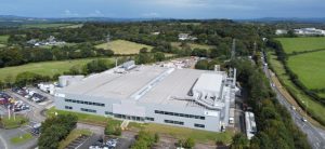
300MM CLEANROOM ACQUISITION OPPORTUNITY
ATREG has been retained to facilitate the disposition of a state-of-the-art 300mm cleanroom facility. The site is located in the western hemisphere and offers improved time to market in an innovation-rich ecosystem. Companies interested in access to a production-ready 300mm asset should contact ATREG’s COO Annie Rothrock for more information.
ATREG FACILITATES PLESSEY’S PLYMOUTH UK 200MM FAB SALE TO HAYLO LABS
ATREG is pleased to announce that it successfully facilitated the divestment of Plessey Semiconductors‘ operational 200mm compound semiconductor fab located in Plymouth, UK to Haylo Labs. Headquartered in London, Haylo Labs is one of the UK’s leading deeptech venture operators with extensive experience in the microLED space. The Plessey facility will continue to operate as an R&D center for the development of display technology, R&D prototyping, and low-volume manufacturing, building on the extensive legacy that Plessey has established in the UK semiconductor industry.
 “ATREG’s deep global semiconductor industry market knowledge proved invaluable in connecting us with the ideal buyer for our Plymouth manufacturing facility,” explains Keith Strickland, CEO of Plessey Semiconductors. “The highly competitive global process ATREG ran brought a broad array of qualified buyers to the table and ensured that the Plessey legacy of semiconductor excellence will continue with Haylo. Most importantly, it provides stability and a long-term future for our employees and the local community.”
Click here to read our full press release.
RECAP OF ATREG’S SEMICON WEST PANEL DISCUSSION
On October 8th at SEMICON West in Phoenix, AZ, ATREG COO Annie Rothrock moderated a panel – Resources for Expanding Operations in the U.S.: Fab Development & Expansion Success Stories – with leaders from some of the world’s most reputable companies in the semiconductor industry:
- Kristin Baldwin Homsi, Manager of Supply Chain, Manufacturing & Technology, at Bechtel Corporation
- Thorsten Scheer, Regional President, Automotive Electronics division, North America, at Robert Bosch GmbH
- Sunil Thekkepat, Vice President, Worldwide Facilities, at Texas Instruments
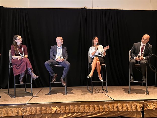 Our panelists shared valuable insights from their experiences with expansion, development, and project execution in the semiconductor space, whether planning new construction, facility conversion, or capacity expansion through existing infrastructure. As the industry works to expand domestic production, this session highlighted real-world examples of successful complex facility projects – from greenfield developments to brownfield expansions and strategic facility transitions – to scale their U.S. operations.
Here are a few key insights from this discussion:
- Brownfield acquisitions can deliver 1.5-year time-to-market advantage through inherited workforce, established utility infrastructure, and existing stakeholder relationships.
- Non-traditional semiconductor locations such as Sacramento can offer superior workforce retention (12+ year tenure) at lower costs than established hubs, making them viable expansion targets.
- Utilities-first planning, digital twin technology, built-in sustainability features, and off-site modular construction can reduce on-site work by millions of hours while enabling faster future expansion.
- Early engagement with community colleges to develop fab-specific curriculum is essential for building the skilled workforce pipeline U.S. expansion requires.
- Greenfield sites adjacent to existing U.S. operations provide the best risk-adjusted expansion path, combining design flexibility with established infrastructure and stakeholder relationships. In other words, targeting brownfield sites with expansion space enables a long-term growth strategy.
Should you have any questions regarding the development of your semiconductor manufacturing operations in the USA, please email our COO Annie Rothrock.
ADVANCED PACKAGING AT A TURNING POINT
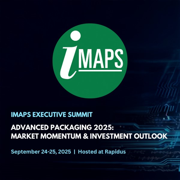 This year’s IMAPS Executive Summit, held on September 24 and 25 at Rapidus in Santa Clara, CA, focused on the market momentum and investment outlook of advanced packaging. Here is a summary of the key insights garnered by the ATREG team that attended the event.
The conference underscored how rapidly the semiconductor industry is being reshaped by the demands of artificial intelligence (AI). Advanced packaging, once viewed as a back-end consideration, is now a central driver of value creation, facility investment, and technological innovation. The event highlighted both the challenges and opportunities of this new era, defined by the convergence of front-end and back-end processes, the emergence of new packaging paradigms, and the need for unprecedented levels of infrastructure development.
A central theme was the fundamental transformation of packaging economics. Advanced packaging has grown from just 10% to 15% of total packaging spend a decade ago to nearly 30% today, with some forecasts suggesting it could reach 50% by the end of the decade. TSMC alone now controls half of global advanced packaging expenditures, doubling its CoWoS capacity annually, yet still struggling to meet demand from Nvidia, AMD, and other AI leaders. Leading OSATs such as Amkor and ASE are reporting margin expansion, but they remain a generation behind foundries and are investing heavily to maintain competitiveness. This dynamic is consolidating power among a handful of players while raising the capital requirements needed to compete.
Another critical shift is occurring in manufacturing infrastructure. OSATs that once operated in Class 10,000 cleanrooms are now being asked to meet standards approaching those of front-end fabs – Class 1,000 or better – particularly for hybrid bonding processes. This represents not just a technical challenge, but a wholesale rethinking of facility strategy. Many existing packaging sites cannot be retrofitted easily and may require complete redesigns or new construction, creating significant opportunities for facility disposition, greenfield development, and partnership models.
Panel-level packaging emerged as one of the most promising new paradigms. Unlike the failed industry push for 450mm wafers, panel-level approaches are gaining traction because they directly address the oversized nature of AI accelerators, which fit more efficiently on rectangular substrates. SEMI has already standardized two panel sizes – 510mm x 515mm and 600mm x 600mm – and leading companies such as TSMC, ASE, Intel, and Samsung are all investing. Although still a small market at $350 million in 2024, panel-level packaging is expected to triple in size by 2030, making it the fastest-growing segment in advanced packaging. Building these facilities requires expertise that spans both semiconductor and display manufacturing, opening new opportunities for specialized consulting and infrastructure services.
 Hybrid bonding, once confined to niche applications, is now becoming mainstream. Already central to CMOS image sensors and high-bandwidth memory (HBM), hybrid bonding allows for unprecedented density in multi-die integration. HBM has particularly emerged as a driver of demand, with 16-die stacks that are reportedly more expensive than GPU chiplets themselves. Technical hurdles remain, such as pad consistency and scaling to printed circuit board integration, but the trajectory toward widespread adoption is clear.
Another frontier is co-packaged optics, which seeks to overcome the limitations of copper interconnects that leave graphics processing units (GPUs) idle as much as half the time waiting for data. Optical chiplets promise far higher bandwidth and lower power consumption, potentially enabling air cooling once again. Companies such as Ayar Labs are pushing forward with technologies such as the TeraPHY optical engine, while TSMC has added silicon photonics to its roadmap. For facility planners, this development will require bridging traditionally separate domains of semiconductor packaging and optical assembly.
The conference also spotlighted the emergence of new manufacturing models. Rapidus, Japan’s state-backed effort to restore domestic leadership in semiconductors, has pioneered an innovative facility design that treats every lot as a “super-hot lot” and embraces single-wafer processing. Its Okido Valley campus, which combines front-end and back-end operations on a single site, has moved from groundbreaking in 2023 to first wafers in 2025, demonstrating remarkable speed.
Underlying all these changes is the unrelenting growth of AI infrastructure. Data centers are projected to consume 8 to 12% of U.S. electricity by 2028, with such hyperscalers as Microsoft and Google investing at unprecedented levels. Compute requirements for next-generation reasoning models are 10 to 100 times greater than before, and the industry is already looking toward system-on-wafer and system-on-panel architectures as Moore’s Law approaches its physical limits. Advanced packaging and algorithmic optimization are the new levers of performance.
 The venture capital (VC) and start-up ecosystem remains a mixed picture. While overall VC funding has quadrupled over the last decade, semiconductors still attract a disproportionately small share – about $2 billion annually – compared to the flood of capital chasing AI software. Governments are stepping in to fill this gap, with U.S. agencies deploying CHIPS Act funds to support early stage innovation. However, challenges remain, including a dry IPO market, limited M&A activity, and an acute shortage of substrate suppliers, with only two major providers globally.
For ATREG, the strategic implications are significant. In the near term, OSAT cleanroom upgrades, panel-level packaging installations, and hybrid bonding facility requirements represent immediate opportunities. Over the next several years, demand will grow for foundry/OSAT partnership facilities, co-packaged optics integration, and second-source manufacturing strategies. Longer term, entirely new architectures – system-on-wafer, glass substrates, and data center-adjacent manufacturing – will redefine the landscape.
The 2025 IMAPS Executive Summit made clear that advanced packaging is no longer the silent partner of semiconductor manufacturing. It is the critical enabler of AI’s future, driving massive investment in infrastructure, materials, and design. For those with the expertise to navigate this transformation, the opportunities are as unprecedented as the challenges.
For any questions on advanced packaging manufacturing, please email ATREG’s Senior Associate Stuart Smith.
SEE YOU AT UPCOMING GLOBAL INDUSTRY EVENTS
 Members of the ATREG team will be attending quite a few global industry conferences until the end of the year. Please don’t hesitate to email us to schedule a meeting with one of our fab transaction advisors at any of the events below to discuss your global manufacturing strategy and infrastructure-rich semiconductor asset needs. Whether your company seeks to acquire or sell a brownfield wafer fab, select the best location for a brand-new greenfield facility, or partner with a third-party for capacity, we can help! Looking forward to seeing you there!
- November 18-19 – Wells Fargo TMT Conference, Palos Verdes, USA
- November 18-21 – SEMICON Europa, Munich, Germany
- November 20 – SIA Annual Awards Dinner, San Jose, USA
- December 4 – GSA Annual Awards Dinner, Santa Clara, USA
- December 17-19 – SEMICON Japan, Tokyo, Japan