


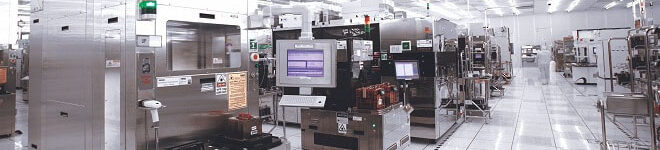
GLOBAL SEMI FABS AVAILABLE FOR SALE As the new year gets underway, momentum is building across the global semiconductor manufacturing asset market. Increased activity and renewed investment interest are creating
More »
GLOBAL SEMI FABS AVAILABLE FOR SALE As the new year gets underway, momentum is building across the global semiconductor manufacturing asset market. Increased activity and renewed investment interest are creating
More »
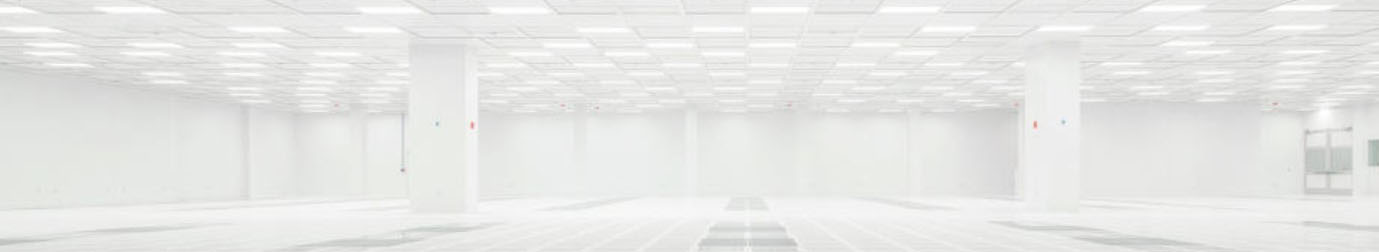
300MM CLEANROOM ACQUISITION OPPORTUNITY ATREG has been retained to facilitate the disposition of a state-of-the-art 300mm cleanroom facility. The site is located in the western hemisphere and offers improved time
More »

EXECUTIVE Q&A: JOHN NEUFFER, PRESIDENT & CEO, SIA ATREG recently sat down with John Neuffer, President and CEO of the Semiconductor Industry Association (SIA) headquartered in Washington D.C., to discuss
More »

350MW SHOVEL-READY GREENFIELD SITE Despite recent market fluctuations, the global semiconductor industry is on an unprecedented growth trajectory and New York State is uniquely positioned to be a leader in
More »

AVAILABLE FOR SALE: OPERATIONAL COMPOUND SEMICONDUCTOR FAB, USA ATREG has been retained to facilitate the divestment of a U.S.-based, state-of-the-art compound semiconductor-capable fab. This facility offers immediate access to more
More »