


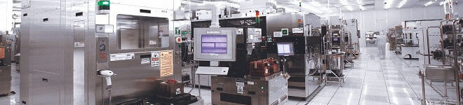
GLOBAL SEMI FABS AVAILABLE FOR SALE
 As the new year gets underway, momentum is building across the global semiconductor manufacturing asset market. Increased activity and renewed investment interest are creating timely opportunities for companies looking to expand or reposition their chip manufacturing capabilities.
Well positioned to support these needs, ATREG currently has a diverse portfolio of manufacturing facilities available for sale worldwide, including a selection of 200mm and 300mm fabs and cleanrooms. Should your company seek to acquire a manufacturing facility in the coming months and be interested in discussing any of our different fab offering opportunities, please email our COO Annie Rothrock to set up a conference call.
IMEC IP LICENSING: TECHNOLOGY TRANSFER OPPORTUNITIES
ATREG partners with imec to assist in licensing a subset of their IP portfolio. For companies looking to supplement their R&D roadmap and expedite new technology development, these technologies – which extend across a variety of industries and applications – offer a unique opportunity.
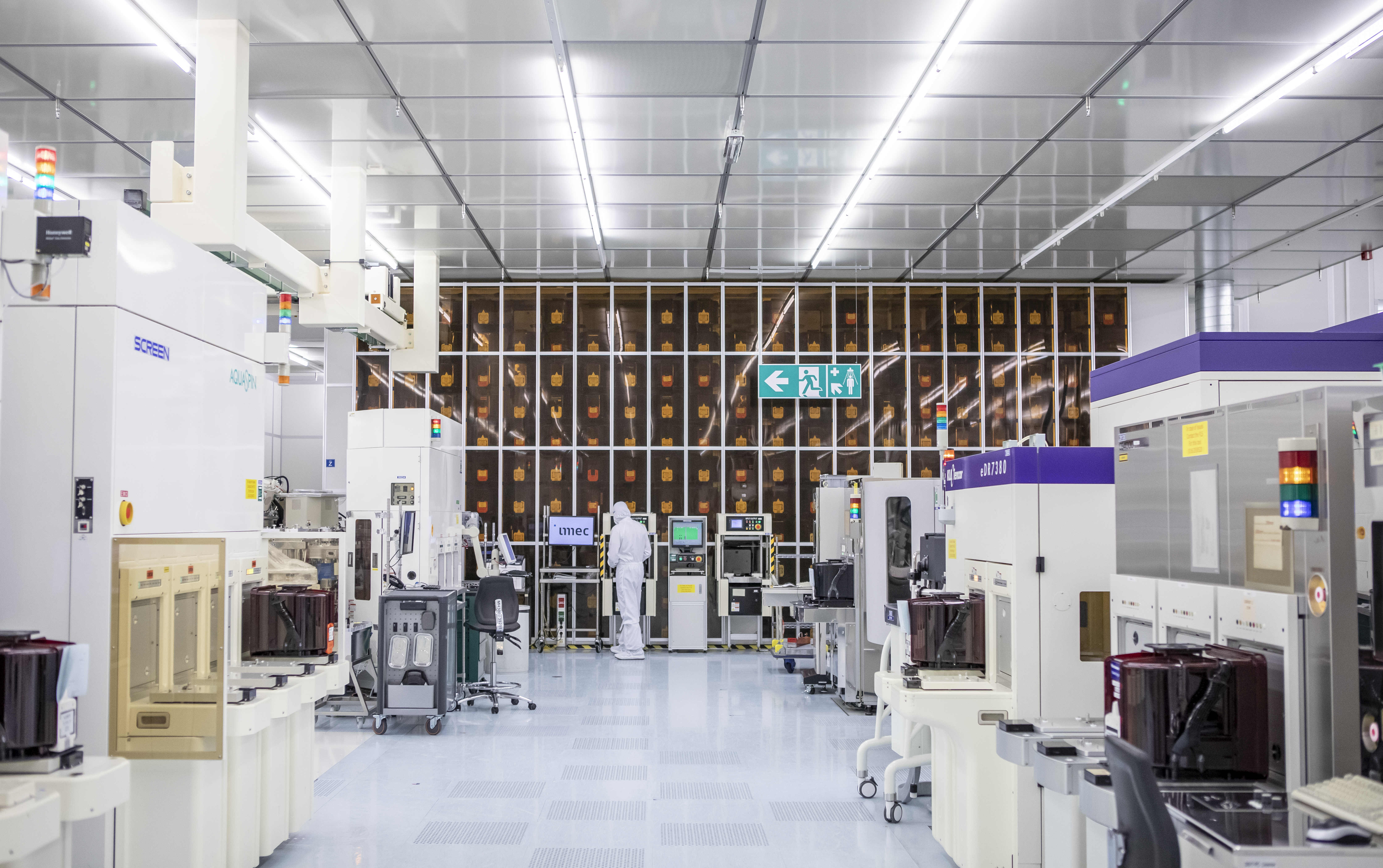
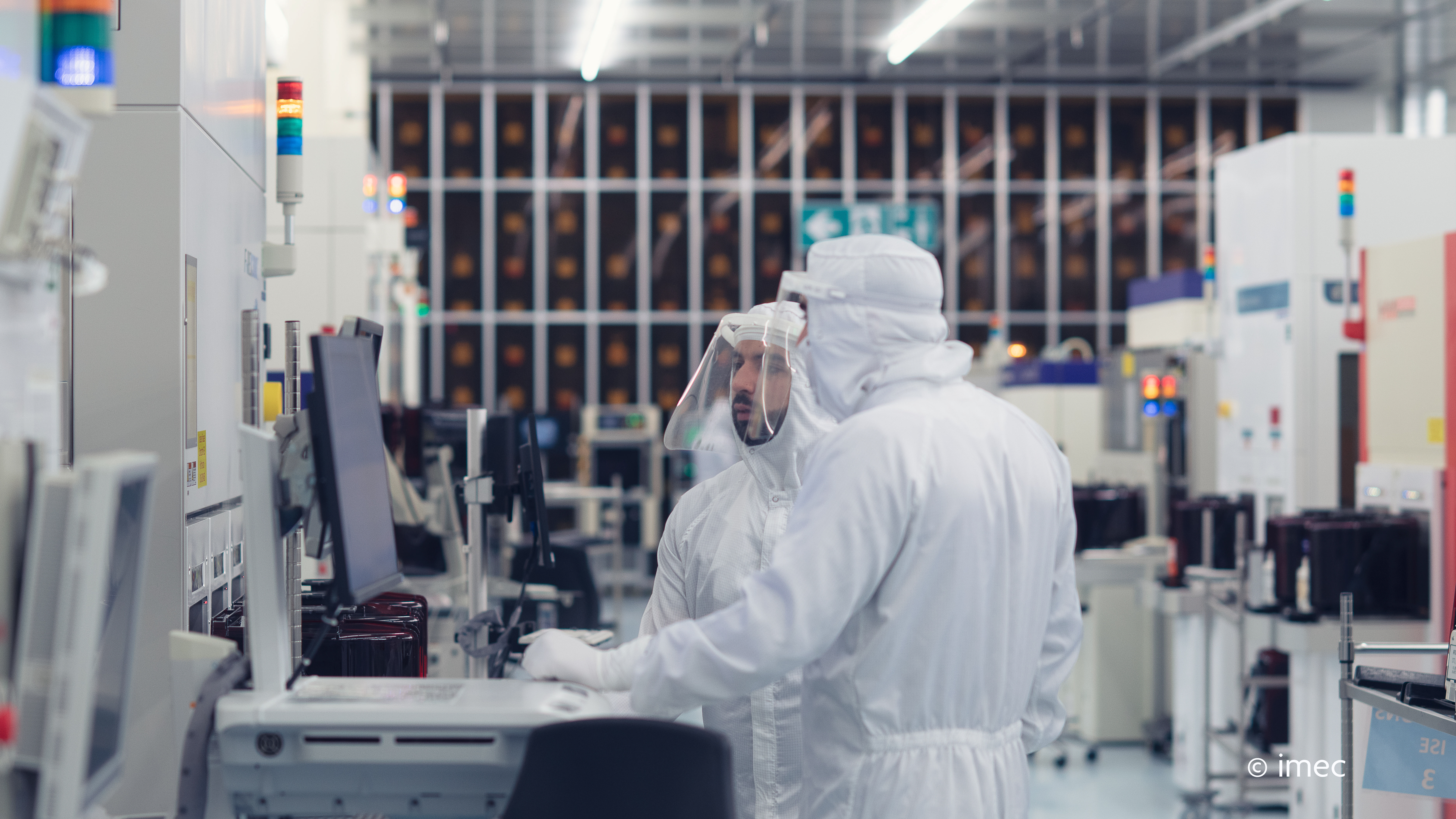
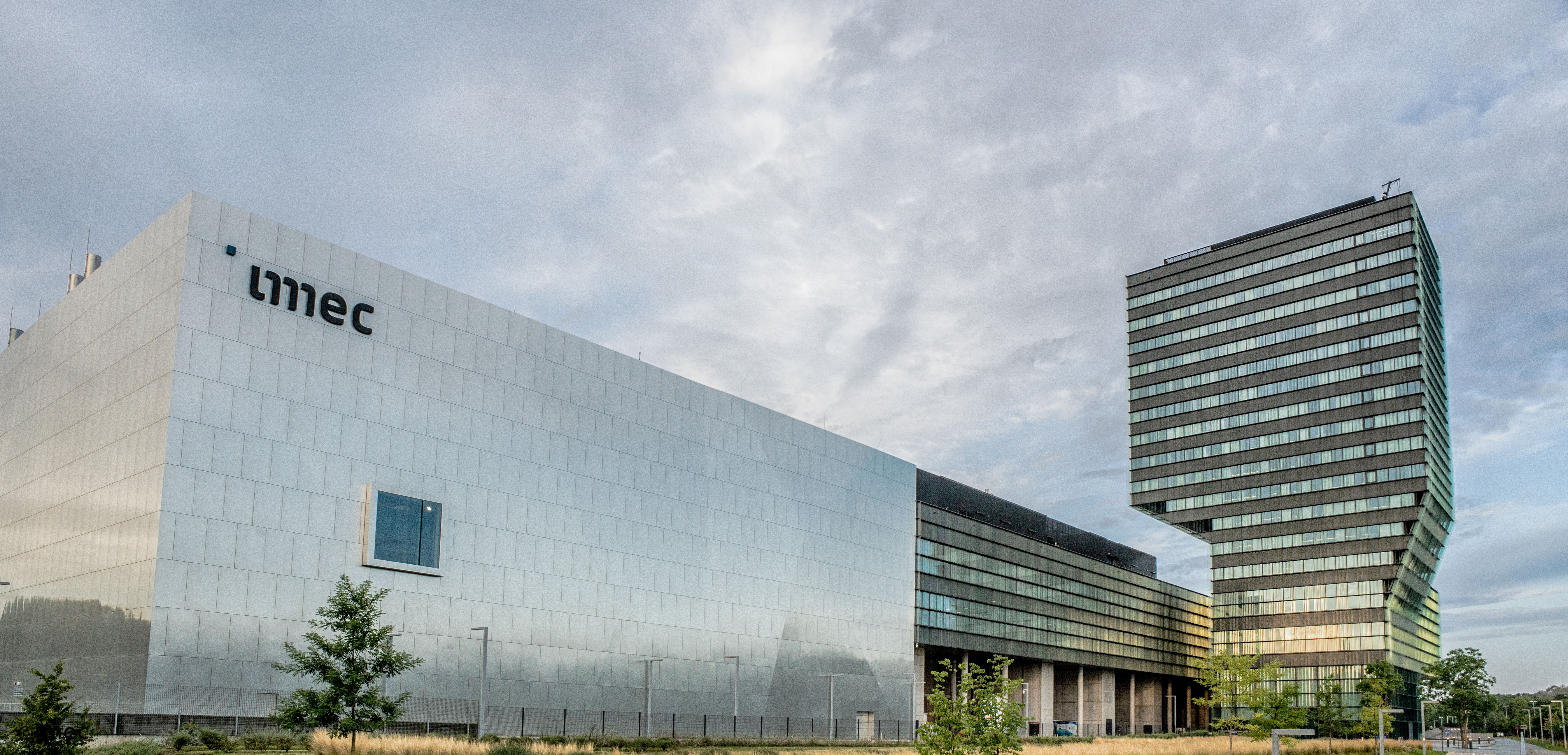 Headquartered in Leuven, Belgium, imec is the world’s leading semiconductor research and innovation hub, with over 6,500 employees and more than 600 industry partners spanning the global chip value chain. The organization operates the most advanced R&D pilot line in the world and has been developing licensable semiconductor technology platforms for over two decades. In December 2025, Taiwan’s UMC became the latest foundry to license imec’s silicon photonics technology for high-volume 300mm production, a testament to the commercial maturity and industry relevance of imec’s IP portfolio.
Licenses include access to imec’s experienced engineering team, which supports technology transfer by training the team of the receiving fab. Through its IC-Link division, imec also offers design and manufacturing services for ASICs, photonic ICs, custom wafers, and advanced packaging.
In addition to helping accelerate R&D cycles, partnering with imec can also provide priority access to future technology advancements.
Available technology platforms
 Silicon photonics platform – For manufacturers looking to capture a portion of the rapidly growing data center opportunity, imec offers a mature silicon photonics platform with co-integrated 200Gb/s building blocks for high-bandwidth optical I/O communication. The technology is production-ready on 200mm and 300mm and compatible with existing CMOS manufacturing processes. The platform includes integration flow, process design kits, characterization methodologies, and documentation. IC-Link also offers manufacturing, design, packaging, testing, and supply chain management services.
- Advanced RF (GaN-on-Si) – imec’s RF GaN platform demonstrates performance on par with the more expensive RF GaN-SiC. It supports supply voltages up to 28V using a 200mm-CMOS-compatible process. The technology features d-mode operation with a HEMT architecture, implements a multi-level copper BEOL and covers frequencies up to 28GHz. Applications include 6G wireless infrastructure, satellite communication, and (X-band) radar. The development of a 5V e-mode MISHEMT and 300mm platform are ongoing, targeting next-generation smartphone and battery-powered edge device applications.
 GaN-on-silicon power technology – imec’s GaN power platforms cover voltage ranges from 40V to 650V, using a 200mm CMOS-compatible process. 40V/100V and 650V are currently available for licensing. The technology features e-mode operation with a p-GaN HEMT architecture and includes manufacturing recipes optimized for AIXTRON MOCVD reactors. 1200V lateral HEMT and vertical MOSFETs are in development, as well as GaN platforms on 300mm. Applications include electric vehicle (EV) charging infrastructure, data center power supplies, and power management systems.
Additional information
In addition to the above, imec offers licensing for CMOS, image sensor, and memory technologies. imec’s approach provides technology modules rather than complete commercial solutions, allowing manufacturers to customize implementations for specific applications while accessing ongoing technical support and development programs.
For more information on any of these opportunities, please contact ATREG COO Annie Rothrock or ATREG Vice President Stuart Smith.
EUROPE’S SEMICONDUCTOR OPPORTUNITY: MEETING THE MOMENT
By Stephen M. Rothrock, Founder & CEO, ATREG, Inc.
![]() What does the future hold for the European semiconductor industry? In this contributed viewpoint published in Semiconductor Digest‘s 2026 Outlook this month, ATREG Founder & CEO Stephen Rothrock reviews the real reasons behind Europe’s semiconductor opportunity.
What does the future hold for the European semiconductor industry? In this contributed viewpoint published in Semiconductor Digest‘s 2026 Outlook this month, ATREG Founder & CEO Stephen Rothrock reviews the real reasons behind Europe’s semiconductor opportunity.
The European Chips Act was meant to be a wake-up call. Three years later, the response has been underwhelming. Intel’s German megafab is on hold, Wolfspeed’s European expansion never materialized, and Broadcom pulled out of their $1 billion plan for an R&D site in Spain. The €43 billion initiative has produced a handful of meaningful commitments – ESMC, STMicroelectronics, Infineon, GlobalFoundries, and Silicon Box, but Europe’s share of global chip production continues to slide.
Yet declaring Europe’s semiconductor ambitions dead would be a mistake. The real opportunity is not about chasing Taiwan’s leading-edge dominance or outspending America’s subsidies. It lies in something Europe already does exceptionally well – specialty and mature-node manufacturing backed by world-class research infrastructure.
 Consider the fundamentals. Europe’s research ecosystem – imec, CEA-Leti, Fraunhofer, VTT – remains unmatched. As imec’s Luc Van den hove has noted, “You can’t make an advanced chip without European technology.” The FAMES Pilot Line, one of five pilot initiatives within Europe and funded with €830 million, is bringing together these institutions to develop low-power technologies for automotive, IoT, and mobile applications. Critically, its open access policy gives European manufacturers early access to next-generation capabilities that competitors simply cannot replicate elsewhere.
Meanwhile, defense spending is surging. Germany has announced plans to double defense expenditure to €650 billion over five years. France, Italy, and the UK are following suit. This isn’t abstract policy – it’s real demand for mature-node chips in missiles, drones, and secure communications systems. Europe’s reliance on Chinese legacy chip production for strategic applications has become untenable, demonstrated forcefully by the recent Nexperia situation.
Policymakers are taking notice. A European Chips Act 2.0 is already taking shape, with EU member states agreeing earlier this year to strengthen their collective position in semiconductors. Unlike the original legislation which offered no specific support for mature-node production, the next iteration is expected to target the legacy chips that underpin Europe’s defense and industrial base. Importantly, European policymakers need to maintain the legacy semiconductor assets they already have and prevent them from falling into disrepair and closure. Whether for leading-edge 300mm applications or such specialty applications as photonics, numerous semiconductor firms globally have found creative solutions to refurbish mature fabs – ADI in Oregon, New Photonics in Belgium, and Octric Semiconductors in the UK are three examples worth replicating.
The strategic calculus is straightforward. Semiconductor companies without meaningful European capacity risk ceding ground to competitors who recognized this shift early. The window to establish presence ahead of the competition is open, but it won’t remain so indefinitely.
ATREG PROMOTES STUART SMITH TO VICE PRESIDENT
 ATREG is pleased to announce the promotion of Stuart Smith to Vice President. Since joining us in March 2019, Stuart has exemplified the excellence and integrity that define our firm. Over nearly seven years, he’s grown from intern to analyst to trusted leader – advancing our semiconductor manufacturing transaction capabilities, driving market analysis, and identifying new opportunities across the globe.
Stuart’s dedication and strategic thinking have been instrumental in strengthening ATREG’s position as a specialist in advanced technology cleanroom asset transactions. As Vice President, he’ll continue expanding his client relationships while leading key initiatives for the firm. Congratulations, Stuart!
SEE YOU AT GLOBAL INDUSTRY EVENTS
 ATREG currently has a selection of 200mm and 300mm fabs and cleanrooms available for sale worldwide. Should your company be looking to acquire a manufacturing facility in the coming months, please email us to set up an appointment with an ATREG fab transaction advisor at one of the following global industry conferences. In addition to brownfield needs, we are available to discuss greenfield fab opportunities and capacity / loading partnerships. We look forward to connecting with you soon!
- FOA Summit (Q1 Collaborative Forum), February 24-26, Austin, USA
- Morgan Stanley Technology, Media & Telecom Conference, March 2-4, San Francisco, USA
- ISIG Executive Summit USA, April 21-22, Silicon Valley, USA
- Display Week, May 5-7, San Jose, USA
- JP Morgan Global Technology, Media & Communications Conference, May 18-20, Boston, USA
- ITF World, May 19-20, Antwerp, Belgium
- Stifel Cross-Sector Insight Conference, June 2-3, Boston, USA
- Bank of America Global Technology Conference, June 2-4, San Francisco, USA
- GSA European Executive Forum, June 10-11, Munich, Germany